This thread has been locked.

If you have a related question, please click the "Ask a related question" button in the top right corner. The newly created question will be automatically linked to this question.

SN74LVC1G17-Q1: Problem with the input and out for the single buffer schmitt-trigger

Part Number: SN74LVC1G17-Q1

Hi dear E2E colleagues,

I try to use the SINGLE SCHMITT-TRIGGER BUFFER SN74LVC1G17-Q1. In my system i use Vcc = 3,3 V. According to the datasheet where i read the take the values for the negative and positive threshold voltage with Vcc = 4,5 und Vcc = 3V, i make the calculation for those threshold for Vcc= 3,3 V. then  i expected maximum 1,518 V for the positive-going input threshold and maximal 1,435 for the negative-going threshold.

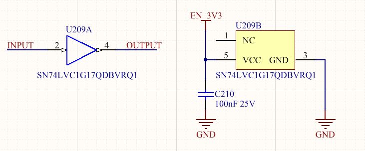
In my circuit i only use a 100 nF as filter for Vcc = 3,3 V. I didn't have any another component.

Problem: The buffer don't work good as expected. I expected Vout = 0V when Vin smaller or equal to 1,435 V and Vout = 3,3 V when Vin bigger or equal to 1,518 V.

Another Problem: I see also exactly the same voltage at the Input and at output in all the range from 0 to 3,3 V. I mind Vin = 1,5V - Vout = 1,5, Vin = 1,8 - Vout = 1,8 etc...

i put the very simple circuit from my shematic for your analyse.

Another Problem: the output voltage swing sometimes to much


I will be very happy to have your answer quicktly as possible

Thank you

  • Hello,

    Your schematic looks fine to me -- 0.1uF (100nF) is the most commonly recommended value for a decoupling capacitor.

    I don't know what you mean by this:

    Another Problem: I see also exactly the same voltage at the Input and at output in all the range from 0 to 3,3 V. I mind Vin = 1,5V - Vout = 1,5, Vin = 1,8 - Vout = 1,8 etc...

    Are you saying that when you put 1V on the input, the output is also exactly 1V? If that is the case, I would check your system for a short or replace the device.

    Using linear interpolation from the nearest 2 points given in the datasheet (3V and 4.5V), I find that the threshold limits are:

    VT+ min, max: 1.502V, 2.04V

    VT- min,max: 0.86V, 1.498V

    deltaVT min,max: 0.432, 1.056

    From these values, the input must be below 0.86V to be guaranteed to be a logic LOW, and above 2.04V to be guaranteed as a logic HIGH.

    Can you provide oscilloscope shots of the input and output signals? (preferably at 100ns/div or faster scale)

    What type of load do you have connected at the output? (usually given as resistance and/or capacitance values to ground)

    What type of signal do you have connected to the input? (source resistance, signal slew rate, frequency of operation, high/low voltages)

  • Hallo Emrys,

    thank you for the Answer.
    Another Problem: I mind, sometimes i see exactly the same voltage from the input at the output.
    i didn't use a load by the test. I measure directly to the output. Ist that a problem? A load should be implement ? With load can I use to do a right test of the component? With values of the capacitors or resistors for the load need to be use? they need to be connect to ground?
    For the signal I only use a power supply and I change the voltage value from 0 to 3,3 V. I used a simple multimeter to measure the output voltage.
    Thank you to the answer

    Alberto
  • Hey Alberto,
    When you measure the output, you are applying a load to it -- most likely it is a very light load from a multimeter of 1 Mohm and just a few pF of capacitance.

    It's ok to test with a power supply as the input. You should be seeing ~0V at the output when the input is low, and ~Vcc at the output when the input is Vcc. We do test every device that we sell for functionality -- and many millions of these devices are used worldwide in a wide variety of applications. I would recommend carefully looking at your test setup for any problems.