Because of the Thanksgiving holiday in the U.S., TI E2E™ design support forum responses may be delayed from November 25 through December 2. Thank you for your patience.

This thread has been locked.

If you have a related question, please click the "Ask a related question" button in the top right corner. The newly created question will be automatically linked to this question.

CD4050B: CD4050 Input & Output characteristics

Part Number: CD4050B
Other Parts Discussed in Thread: UCC27527, CD40106B

Hi

I had asked a Q reg UCC27527 Input characteristics .

This is a related Q 

We want to create a Short Pulse Suppression Ckt for our 0-15 V Signals from the DSP 

Typical value would be 930 nS with guaranteed values for Min & Max .

We want to use CD4050 as per the following Ckt 

Basically it Shifts the Input Pulse Train in Time Domain while killing shorter pulses .
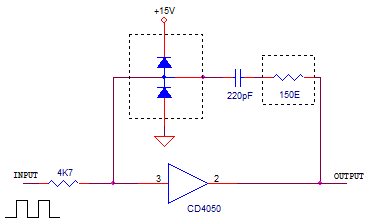
Question is whether we need those Voltage Clamping Diodes and the current limiting Resistor ? 

Thanks and regards

Varunesh

  • Hey Varunesh,

    First - thank you for separating this question from the other thread - this helps us significantly with issue tracking, it helps me to understand the issue, and it helps anyone who has a similar question regarding the CD4050 in the future.

    -----------------------------

    To directly answer your question, I would recommend keeping the diodes. You might also have some trouble with excessive current and oscillations from the slow inputs. More details follow.

    -----------------------------

    The circuit shown will typically work, but there are a couple of important issues:

    (1) The input RC circuit (4.7k + 220pF) produces a very slow edge into the device. This will produce excessive current and could possibly start oscillations as explained in this FAQ:


    Just removing the resistor won't solve the issue - it will just mess up the timing you have configured. The whole point of the circuit is to have a slow input to produce a delay.

    The only fix I know of for this would be to switch the device for a Schmitt-trigger inverter that is designed to have slow inputs, for example, the hex schmitt-trigger inverter CD40106B. Two channels can be placed in series to produce a Schmitt-trigger buffer.  Unfortunately, we don't have a ST buffer that supports 3-18V operation.

    (2) When the device switches, there will be a sudden jump of the input voltage -- which is why you have the suppression diodes and I assume the reason you are asking this question is to determine if the CD4050's internal clamp diodes are good enough to suppress this event on their own.

    The internal diodes of the CD4050 won't react fast enough to prevent damage if the voltage spikes go as high as I would expect (up to ~1.5x Vcc or 22.5V, which is larger than the abs max voltage rating fo the device). For fast changing signals, we always recommend an external clamp diode, preferably at a lower voltage than the internal diodes to prevent them from turning on at all.

    If this answers your question, please click the green "this resolved my issue" button; or if you need additional assistance, just respond to this thread.

  • Hi Emrys 

    Thanks for your prompt response .

    Yes ; I too was concerned abt the slow moving Inputs on its Input Pin .

    Yes ; CD40106 does work and if you see the earlier thread ; I had put up its waveforms .

    We have now a toss up between UCC27527 & CD40106 ; and methink we would opt for the 

    former with clamping diodes and the Series Resistor .

    When cost optimization is reqd ; maybe CD40106 with a Emitter follower BJT pair .

    Although my issue is resolved ; would appreciate receiving your comments reg CD40106 

    O/P drive capacity being boosted by an Emitter Follower BJT Pair .

    Since we are working with +15 V Levels ; the 0.6V Low Level ( & 14.4 V Hi ) with BJT Emitter Follower

    Pair is of no major concern .

    Thanks again for your very prompt response 

    Rgds 

    Varunesh