Part Number: SN74LVC1G125
Hi all
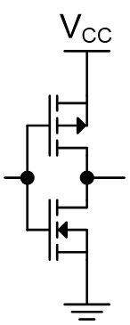
While looking at the SN74LVC1G125 Datasheet I come across comments in section 10.2.1 (copied below).
Can you elaborate on the implications ?
Can you provide a functional block diagram and a detailed description of the architecture of the output stage ?
Thank you for providing feedback
Ueli
----------------------------------
10.2.1 Design Requirements This device uses CMOS technology and has balanced output drive. Care should be taken to avoid bus contention because it can drive currents that would exceed maximum limits. The high drive will also create fast edges into light loads so routing and load conditions should be considered to prevent ringing.