This thread has been locked.

If you have a related question, please click the "Ask a related question" button in the top right corner. The newly created question will be automatically linked to this question.

TXB0108: TXB0108 output at high load capacitance

Part Number: TXB0108
Other Parts Discussed in Thread: TXS0108E, SN74AXC8T245

Hi Tiers.

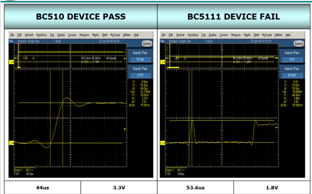
My customer already using TXB0108.

In order to Signal line is so long and capacitive load increases, B side output level is about 1.5V at one shot operation. (desired 3.3V)

They have to use TXS0108 in this situation? or Do you recommend other part?

They want pin to pin alternate part.

  • The TXS0108E is the only P2P part, and it might work, if the speed is not too high.

    (In general, a fast translator with automatic direction sensing cannot be used with a high capacitive load.)
  • Thanks.

    I have new questions.

    I attached waveform image.

    left is normal operation(3.3V), right is abnormal operation(1.5V).

    B side signal pcb trace length is about 400mm.

    My customer want to know that.

    1. According to the note "A Guide to Voltage Translation With TXB-Type Translators",

    even if mos TR is turned off, I think it will go up to 3.3V according to RC time.

    Please let me know some the reason to stay at 1.5V.

    2. And let me know how is the OS turn off operation.

    3. How can fix this? let me know solution? (add series resistor? add PU or PD resistor?)

    4. If TXB0108 is swapped TXS0108E, is this solution? (TXB0108 is push pull type.)

    [ Contents of "A Guide to Voltage Translation With TXB-Type Translators" ]

    With regard to capacitive loads, TXB translators are designed to drive up to 70 pF without issue. If

    capacitive loading is larger than 70 pF, the O.S. will time-out after 10 ns and subsequently turn off before

    the output voltage is driven fully high or low. From there, the output will continue to rise or fall based on

    the RC time constant determined by the 4-kΩ buffer, load resistance and capacitive loading. To ensure

    reliable operation, system designers should keep capacitive loading for the TXB-type devices to 70 pF or

    less. With no external loading, the one-shot circuits will remain on for approximately 4.5 nsec. The

    duration of the one-shots is related to the output voltage level. The output high voltage at which O.S.

    switches off is approximately 95% of full scale, while the output low voltage at which O.S. switches off is

    approximately 5%.


  • If the TXB is the only device driving the line, then the voltage should eventually reach 0 V or 3.3 V. So this looks as if some other device is affect the line; this could be another TXB pin, or some pull-up or pull-down resistor, or some other driver.
    Please show a schematic of everything that is connected to this line.
  • Hi Jake,

    For long traces and capacitive loads, TXB0108 may not be ideal device. You would probably have to consider using a strong buffered driver device like the SN74AXC8T245 which can support 1.5V to 3.3V operation.
    The OS circuit, as you have rightly mentioned in the post times out either around 10ns or 95% of Vcco whichever occurs first.