A related question is a question created from another question. When the related question is created, it will be automatically linked to the original question.
If you have a related question, please click the "Ask a related question" button in the top right corner. The newly created question will be automatically linked to this question.
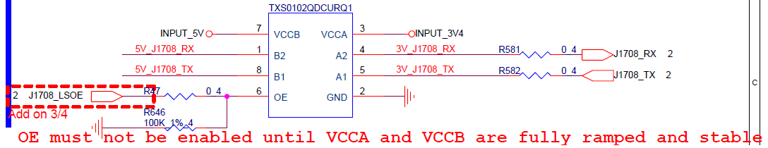
This schematic looks fine. The only comments I have are:
- The R47 and R646 resistors must bias the OE pin high relative to VCCA to enable the I/O pins
- To clarify on the OE pull down: A pull down on the OE pin is recommended to guarantee that the I/O pins will be in a high impedance state during the process of VCCA and VCCB ramping up. Since this device has VCC isolation, the A pins will be hi-Z while VCCB is 0 V, and the B pins will be hi-Z while VCCA is 0V. Not using the pull down may result in extra power consumption while VCC is ramping, but the device will not be damaged.