This thread has been locked.

If you have a related question, please click the "Ask a related question" button in the top right corner. The newly created question will be automatically linked to this question.

SN74AVC4T774: DIR setting requirements and 3-state I/O interface.

Part Number: SN74AVC4T774
Other Parts Discussed in Thread: SN74AXC4T774

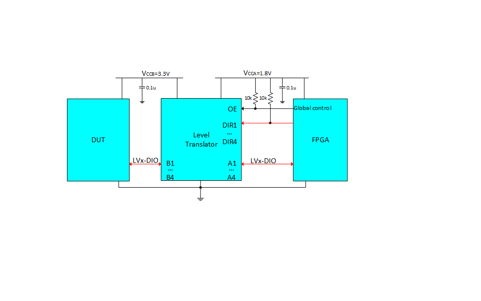
See the schematic above. SN74AVC4T774 is used for voltage shifting from 1.8V to 3.3V.

The requirements of this design proposal:

1. Bandwidth: >50MHz, so >100Mbps.

2. 1.8V is set as the same as the FPGA support voltage. But the VccB should be able to configured for I/O standards from 1.2V to 3.3V.

3. Bidirectional: Independent channel direction control.

4. Interface: 3-state is required in the data chain, because the DUT is unknown. Thus, it can be configured for PU or PD by DUT. The PU/PD resistor is not allowed in the Level translator.

SN74AVC4T774 is available for high speed >100Mbps, 1.2V-3.3V voltage range, individual DIR control pin. Only one OE pin for high-Z set High before power up/down completed.

Requirements 1&2 is OK, but there are some QUESTIONS in 3&4:

3: My design need to read the information back during the data transfer. Thus, the direction will be changed during the running.

In some TI's datasheet, the level shifter with DIR control pin. The device required to disable the device at first, then set the DIR, after this enable the device again. Is it necessary to enable and disable the SN74AVC4T77? Can I set OE to LOW during the normal operation, then during the running, I set the DIR for bidirectional functions without any limitation?

4. I saw some discussion in the forum, the input is always active. Thus, the PU/PD is required for the SN74AVC4T774. Is this used for low power consumption?

But for my design, as we talked before. The logic level should be set by the unknown DUT. It can be High or Low. We can not make a PD/PU on the Level translator.

The worst case will be: direction from DUT to FPGA (B-A), DUT is no signal maybe floating (software maybe can set it for LOW for idle), no PD/PU on SN74AVC4T774. Will this be a big problem?

Kind regards 

Rongpeng Zhai


  • Hello,

    I would first like to begin with switching you from the SN74AVC4T774 to the SN74AXC4T774. These devices are pin to pin compatible. The AXC device is faster than the AVC device so it is a better option for you. It also operates at lower voltages in case you might need this.

    Your schematic did not post, can you please provide it again?

    3: It is necessary to disable the AVC device before switching direction. This is because if A side is driving low or high, and direction pin switches from B to A. Then the AVC device would have to fight the device that is driving the A pin low. Now, if you leave the A pin floating when you switch from B to A, then in the time the direction switches, there will high current consumption. The solution is to use the SN74AXC4T774. You just have to make sure there is no signal on the input of the device before changing direction.

    4. Again with the AXC device, if there is no signal or maybe floating, it should be fine. It has some weak internal pulldowns that will help reduce current consumption that is present with CMOS inputs.

    Overall, recommend using the SN74AXC4T774 as it will solve your issues.

    Thanks!

    -Karan

  • Hi Karan,

    Thanks for your recommendation. There are still some question not clear:

    1. Check the datasheet, AXC is up to 310Mbps < AVC up to 380Mbps. Why you said AXC is faster?

    2. Can you point out where the datasheet of AXC states that "make sure there is no signal on the input before changing direction"? Why it is not required to fight the device that device that is driving the A pin low? And do you talk about the signal direction conflict here?

    and what you mean for no signal? like input is from FPGA, the FPGA is not powered or the input pin is floating?

    3. There is still no spec for DIR change delay.

    int state t1: OE=LOW, DIR=LOW, B to A.

    t2:OE=LOW, DIR=High, A to B.

    t3: OE=LOW, DIR=High, received signal A at B port.

    What is the tD=t3-t1?

    Still calculated by minimum pulse width?

    This is important to know for software to design the rewrite code, etc.

  • Hello,

    1. The AXC is better for the lower voltages, did not intend to say faster.

    2. We don't mention that in the datasheet because the recommendation is to disable the AXC device with the OE pin and then changing the direction. This is the recommendation because there may be bus contention when one side is still driving and the direction gets switched. What I mean by no signal is a floating. If you A side is driving from A to B. Then before changing direction B to A, you should make sure that A goes to floating so that there is no bus contention.

    3. As for delay of direction pin. You can take it to be worst case of disable time plus worst case of enable time of device. These values are listed for the OE pin.
    So tD <= tdis + ten.

    Thanks!

    -Karan

  • Hi Karan,

    Thanks for your help.

    May I ask one more question?

    I think both AVC and AXC's recommendation is to disable the AXC device with OE then change DIR.

    Now, you statement is AXC allows change DIR without disable the device when we make there is no signal. But this is not available for AVC!

    Am I correct? Or it is also ok for AVC, if we make sure there is no signal?

    Thanks!

    RonZha

  • Hello,

    Yes both recommendation is to disable with OE before change DIR.

    AXC has weak internal pulldown while the AVC device does not.

    You will have a large current draw on the AVC device if there no signal (no signal means floating).

    Thanks!

    -Karan

  • Hi Karan,

    Thanks for your help.

    As your suggestion, we selected SN74AXC4T774 as a low voltage level translator.

    During the design, we find a new problem.

    It is easy to make a bus contention when software using the product:

    A side is set to 0, driving from A to B.

    B side is set to 1, driving from B to A.

    Thus, the B side high voltage will be shorted to GND. It seems to burned the device, if the current Is too high.

    Does SN74AXC4T774 has some protection or solution to reset for bus contention issue?

    Thanks for your reply.

  • This level shifter always has a specific direction on each channel, so the output driver on one side is active, and the other device connected to this signal line must not drive it at the same time.

    To disable the output drivers on both sides, set OE low.

    This is not specific to this AXC device; any buffer would have this problem. If the other two chips were using the same voltage, and you had connected them together without a level shifter, you would have the same problem.

  • Hi Clemens,

    Yes, we know that it must not drive the output at the same time. One for 0, another for 1.

    However, there maybe some new software use this product, and make a bus contention.

    So, we need to know what will happen to the device. What will be damaged?

    We want to know the risk of the worst case.

    Thanks.

  • Hi,

    This is what we had discussed before, if the device is going to switch direction, and if there is a chance of bus contention, then the safety mechanism is to use the enable pin clemens has mentioned. It is hard to say what will happen to due to this excessive current but it is very likely that the device will be damaged.

    Thanks!

    -Karan

  • If and output is driven to a different voltage by another driver, then the current through the output transistor is likely to exceed the absolute maximum rating, and burn the chip up.

    If you expect that this can happen, then you should add series resistors to limit the possible current; 150 Ω keeps the current below 25 mA.

  • Hi,

    Thanks for your reply.

    I understand your answer now. Unfortunately, the level-translator is used for high speed line. Thus, the series resistance should not be higher than 50 ohm.

    The output is able to be driven to a different voltage by another external driver. 

    A good news is for normal operation, drivers on both sides are set as 12mA drive strength. 

    Thus, it should be ok when the bus contention happens.

    Thanks for your time.