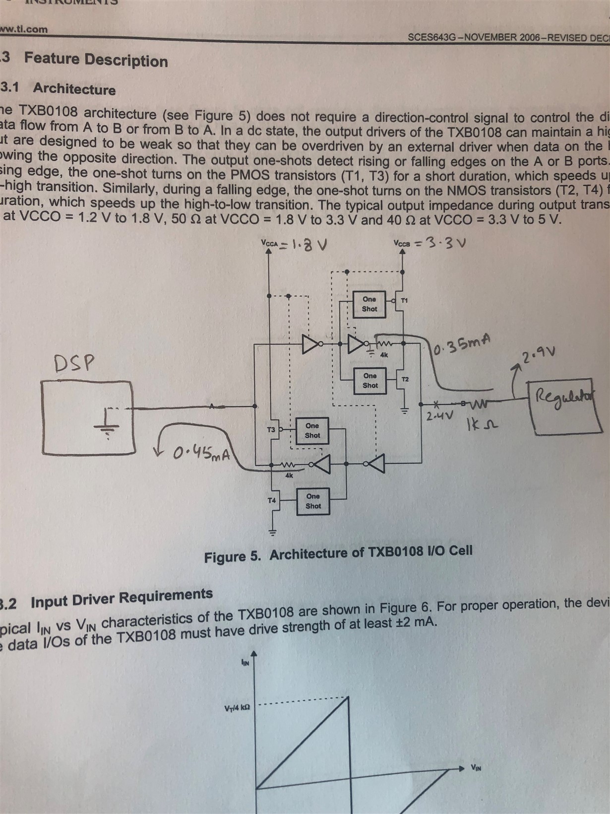
I have a query related to TXB0108 8 bit bi-directional level shifter which we have used in our initial build. We are using output of a regulator (2.9V) to drive one of the i/o of a DSP chip which operates at 1.8V and we have used the txb01018 for the conversion.
The issue is the current gpio we are using is by default setup as output and we program it as input on in the DSP firmware. So at the time of boot up the GPIO comes up as output and is driving as low till the DSP firmware comes up and changes it to being input. This duration is in 100’s of ms. During that duration the B5 ( higher VCC side of level shifter) is being driven by a regulator (2.9v) through a series resistor, while the A5(lower VCC side ) is being driven by the DSP as low till this gpio is programmed as input. In this duration both the pins of the level shifter are being driven in opposite polarity. We want to understand if this brief contention will fail/damage the level shifter? Right now we are seeing that at the time of bootup, at B5 we see 2.4V briefly and then goes back to being 3.3V once I/O is set as input. This 2.4V is drop because of 1K series resistor we have between level shifter and the regulator and internal4k resistor inside level shifter( attaching picture below). Functionality wise we have validated it and it is working as expected once the gpio is programmed. Our worry is the brief contention will damage or fail the level shifter.
For now we want to continue using the same board while we do respin on our board later with proper changes, since this is time critical. We want to continue using the same board with BOM change till we change the board design.
As per our calculations for the brief time 0.36mA will flow though the 4Kohm on VCCB side, and on Vcca side 0.45mA from the inverter through 4k. We think it should be ok but want to get your validation.


