This thread has been locked.

If you have a related question, please click the "Ask a related question" button in the top right corner. The newly created question will be automatically linked to this question.

pin1 orientation on underside of physical component package, mechanical package feature question


What is the actual material of the small pin one square, underside orientation marking on the package near pin 1 for part number SNJ54LVCH244AFK. Is that paint? an indentation?, or is it a conductive material , is it common to pin1? or is it GND? Does it need to be soldered to the PCB? Thanks, Part number was unrecognized in this forum requirement for Part Number.

  • Mark,

    I need to request access to the package drawings to answer this conclusively.

    I will reply back as soon as I confirm.

    Regards,

    Wade

  • Mark,

    After further review, it appears that the package outline drawing that is included in the datasheet is somewhat generic.

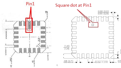
    The square dot represents a pin one indicator.  However, it physically does not represent the package.

    Here is comparison of package outline and package drawing:

    To accommodate the generic pinout drawing to multiple package variation, the following statement is being considered to be added to the outline drawing.

    Pin-1 may be designated by an elongated pad or separate indicator.

    If this answers your question, please click "This Resolved My Issue"
    Regards,
    Wade