This thread has been locked.

If you have a related question, please click the "Ask a related question" button in the top right corner. The newly created question will be automatically linked to this question.

SN74AHC1G86: The input protection circuit (ESD diode) characteristic on SN74AHC1G86

Part Number: SN74AHC1G86

Hello support team,


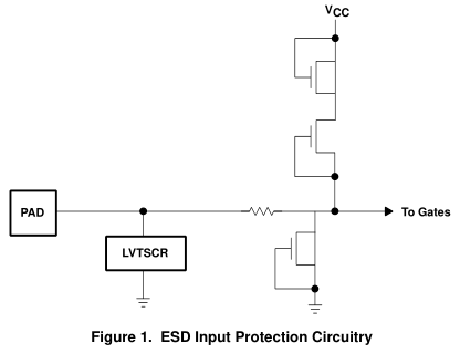
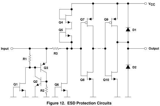
The customer want to know the input protection circuit (ESD diode) characteristic on SN74AHC1G86.

Is the input protection circuit can clamp the plus direction over voltage and also the negative direction over voltage?

The customer needs to know how much current is allowed to both directions and also needs to know how long time is allowed. (Allowed pulse width.)


Because on the customers system the input voltage may have a possibility to go less then GND voltage (go to minus voltage) then asked.


I think in case of above the customer should need to add the clamp circuit externally but not sure the exact things. Please give us your feedback.


Best regards,

Izumi Maruyama


  • See the absolute maximum ratings.

    For negative voltages, there is a diode between GND and the pin. A current of 20 mA is allowed continuously, so there must be a mechanism to limit the current, such as a series resistor.

    Positive overvoltages larger than 7 V are not allowed (except for ESD events, but those have higher voltage and less energy than any signal). If you have positive overvoltages, you need to clamp them with a diode to VCC, or with a Zener/TVS to GND.

    The application note Advanced High-Speed CMOS (AHC) Logic Family (SCAA034) says:

    Electrostatic Discharge

    ESD occurs when a buildup of static charges on one surface arcs through a dielectric to another surface that has the opposite charge. The end effect is the ESD causes a short between the two surfaces. These damaged devices might pass normal data sheet tests, but eventually fail. The input and output protection circuitry designed by TI provides immunity to over 2000 V in the human-body-model test, over 200 V in the machine-model test, and over 1000 V in the charged-device model test.

    Figure 1 shows the circuitry implemented to provide protection for the input gates against ESD. The primary protection device is a low-voltage-triggered silicon-controlled rectifier (LVTSCR). During an ESD event, most of the current is diverted through the LVTSCR. Additional protection is provided by the resistor and secondary clamp transistors, which break down during an ESD event and protect the gate oxides.

    Furthermore, section 2.3.1 of the AHC/AHCT Designer's Guide (SCLA013) says:

    Figure 12 shows protective circuits used for advanced high-speed CMOS devices. To meet the requirements outlined previously, the protective circuit is constructed in two stages. The input is first protected by a thyristor consisting of transistors Q2 and Q3. This provides coarse protection. If the input voltage rises above about 15 V, transistor Q1 breaks down and fires the thyristor. The latter then short circuits the high currents. Resistors R1 and R2 have values of only a few ohms. Therefore, the holding current of the thyristor is several tens of mA. When the current is reduced again at the end of the discharge, the thyristor is extinguished. Transistors Q4, Q5, and Q6 operate as fine protection and are intended principally to protect the input from excessive voltages. When there are overvoltages at the input, these transistors are driven into breakdown and limit the voltage, while resistor R3 limits the current.