Team,
My customer has the following clarification question:
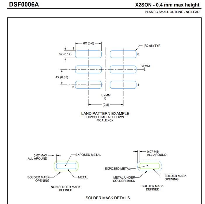
I am working on creating a solder mask defined land pattern for part SN74LVC1G04DSFR. When looking at a land pattern example in the datasheet (image also below), I wanted to clear up a question I had. I believe I made the right assumption, but I don't know for certain if I am correct.
In this image, we are given a Land Pattern Example that is clear in how it is defined. However, I am not certain on the solder mask details. For the non-solder mask defined details, it is clear that the exposed metal definition has the same dimensions as the land pattern example, and the solder mask opening has an extra offset of 0.07 max all around. The solder mask defined pattern is a little less clear. Should I assume that the dimensions from the above "Land Pattern Example" apply to the solid green solder mask opening, or to the dashed blue metal under solder mask?
Thanks!
Aaron


