Part Number: SN74AVC4T245
Other Parts Discussed in Thread: SN74AXC4T245
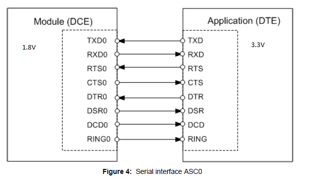
please find the below image. i have my schematic as well as directions of module. i think there is a mistake in level converters direction configuration. please help me make the changes