This thread has been locked.

If you have a related question, please click the "Ask a related question" button in the top right corner. The newly created question will be automatically linked to this question.

LSF0102: LSF0102 output current with no Pullups on Port A

Part Number: LSF0102

Hi all,

I'm using the LSF0102 as a bidirectional level shifter from 1V8 (port A) <-> 3V3 (port B). Unfortunately I've left out the pullup-resistors on the A-port, although the A-port is an output in some cases and I expect currents per channel of ≤ 1mA.
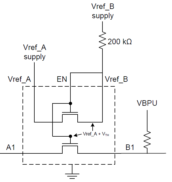
My questions:

Is it possible to increase the current for the logic '1' by decreasing the resistance of the pullup resistor of VREFB (default: 200k) and thereby increasing Vgs (and thus the threshold), so that the NMOS can drive 1mA @ Vout = VrefA without damaging the device?

And for my understanding:

If this is not possible, the voltage on port A will drop during a logic '1', equally Vgs will increase, causing the resistance of the NMOS to decrease and current can flow from port B to A.
So in this case, I expect the voltage drop to be small (< 0.3V)?!

  • Hi Julian, and welcome to the forums!

    The first point of confusion I typically see with the LSF is that it contains 4-port FETs. The Source and Drain are defined by voltages at A1 and B1 - and these can switch during operation. The lower voltage between V_A1 and V_B1 is considered the Source.

    I'm not really sure what you mean here:

    If this is not possible, the voltage on port A will drop during a logic '1', equally Vgs will increase, causing the resistance of the NMOS to decrease and current can flow from port B to A.
    So in this case, I expect the voltage drop to be small (< 0.3V)?!

    If the voltage at the input (A1) is Vref_A and we assume that the nFET is on, then the voltage at (B1) will attempt to follow the voltage at Vref_A, so both sides of the nFET will be ~Vref_A. In this case, is the device on or off?

    Condition for cutoff: Vgs ≤ Vth

    Node voltage at gate: V_gate ~= Vref_A + Vth + V_OD

    ** V_OD is the overdrive voltage required in the bias circuit to provide the ~5uA of bias current

    Vgs = V_gate - Vref_A = Vref_A + Vth + V_OD - Vref_A = Vth + V_OD

    So, technically the device is on, but it cannot supply more than ~5uA of current (the bias current). Considering that the pull-up resistor can provide mA of current, it easily overpowers this and drives the line to VBPU

    **

    For a short explanation, positive current at the B-side is supplied by the pull-up resistor, not the LSF device. Decreasing the pull-up resistor value (not the 200kohm bias resistor) will provide additional drive current. There's a video that discusses this in detail located here: 

    I would recommend watching the full video series on the LSF voltage translators for a detailed explanation (the whole series is under 20 minutes) - far better than anything I could write here.  If you have specific questions after that, please come back and post them - I'll try to help.

  • Thank you for your fast reply!

    A prototype board has already been made, but has not yet arrived and I have just noticed this mistake (missing pullups on A-side). Therefore I want to check some possiblities to get the circuit working before.

    I tried to mark the currents and voltages in the image attached to - hopefully - better describe what I mean.


    In my case A1 is the output (sink) and B1 is the input driven by a gpio (source). Because I left out the pullups on the A-side, the whole current has to be provided by the gpio / source - there is also an example application for this case in the datasheet (p.15, figure 8).
    But the drawn current on the A-side of about 1mA is to high in case the output voltage at A1 is equal to Vref_A and there are no pullup resistors; so the output voltage will drop on the A-side (because the nFET is high impedance), am I right?

    However when it drops, Vgs (marked) increases, so the resistance of the nFET will lower until the drawn current can be provided? If this is correct, maybe the output voltage will still be high enough and I don't have to do anything.

    But if the voltage-drop is to high, my idea was to change the 200k bias resistor to a lower value and thereby increasing V_OD to get a higher bias current (VRef_B - Ibias*Rbias = Vref_A + Vth + V_OD). Is this possible?

    Thanks!

  • Thank you for your fast reply!

    A prototype board has already been made, but has not yet arrived and I have just noticed this mistake (missing pullups on A-side). Therefore I want to check some possiblities to get the circuit working before.

    I tried to mark the currents and voltages in the image attached to - hopefully - better describe what I mean.


    In my case A1 is the output (sink) and B1 is the input driven by a gpio (source). Because I left out the pullups on the A-side, the whole current has to be provided by the gpio / source - there is also an example application for this case in the datasheet (p.15, figure 8).
    But the drawn current on the A-side of about 1mA is to high in case the output voltage at A1 is equal to Vref_A and there are no pullup resistors; so the output voltage will drop on the A-side (because the nFET is high impedance), am I right?

    However when it drops, Vgs (marked) increases, so the resistance of the nFET will lower until the drawn current can be provided? If this is correct, maybe the output voltage will still be high enough and I don't have to do anything.

    But if the voltage-drop is to high, my idea was to change the 200k bias resistor to a lower value and thereby increasing V_OD to get a higher bias current (VRef_B - Ibias*Rbias = Vref_A + Vth + V_OD). Is this possible?

    Thanks!

  • Section 1 of the application report Voltage-Level Translation With the LSF Family says that, without an A-side pullup:

    During the weak 1 condition, TI recommends only high-impedance loads because very small amounts of current will cause the output voltage to drop significantly.

    What exactly do you have connected to A1?

  • Hello Clemens,

    I've read the application report, but too late... For this reason I'm looking for a way to temporarily fix this error as described above.

    A reset pin of a module and a enable pin of a voltage regulator are connected to this pin.

    1mA will probably be more than the circuit actually needs, but the maximum drawn current can be more than 100µA per device - according to the datasheets.

  • Hey Julian,

    Thanks for clarifying. Yes, you can increase the current throughput the way you describe.

    One common issue I see in systems with the LSF is that the supply used at Vref_A often cannot sink current (for example, an LDO) and goes into disregulation. You might have to add a load resistor to sink that extra current at the output of your supply depending on your system configuration.

  • A leakage current of 100 µA would be extremly uncommon for a CMOS input. Are there integrated pull-down resistors, or can you tell us the actual chip numbers?

  • You're right... it's 100nA and not 100µA... so I probably won't get any problems. Nevertheless, I did a spice-simulation to check the approximate behavior: even if the current consumption is about 0,2mA, I expect a voltage drop of 0,3V, which is not a problem.

    Thank you both for your support!