This thread has been locked.

If you have a related question, please click the "Ask a related question" button in the top right corner. The newly created question will be automatically linked to this question.

TXS0108E: Can I use VCCA = VCCB, but powered by seperate regulators?

Part Number: TXS0108E
Other Parts Discussed in Thread: SN74AXC8T245, TXB0108

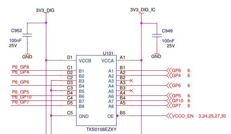
I'm using the device as a buffer between an external GPIO connector and an FPGA. The FPGA and VCCA are both powered by 3V3_DIG_IC, which is internally generated on the board and is nominally 3.3V, and should be reasonably accurate (within 1 or 2%).

VCCB and the external GPIO are powered by an external power supply that can be 3.3V +-0.3V. Obviously this can create a situation where VCCB could be 3.0V, and VCCA= 3.3V. I have the option to lower 3V3_DIG_IC to 3.135V, but can't really go lower than that.

The datasheet gives no tolerance for VCCA being higher than VCCB, so is there any safe value for VCCA to go higher than VCCB, even if it's as low as 0.135V, or will this be enough to damage the device?


  • Hi,

    Welcome to e2e.

    Vccb >=Vccb is the required condition for the TXS0108e device. Going higher than Vccb by 0.5V can draw large currents as mentioned in the biasing requirements for TXS device app note here below:

    http://www.ti.com/lit/an/scea060/scea060.pdf

    But within the tolerance of 3.3V, I would say its definitely not going to damage the device and that the current consumption is not going to be large. 

    curious to also understand why both the supplies are at 3.3V and is there no translation?

  • Thanks for the reply, it seems to confirm that I should be OK.

    There are a few reasons to use the buffer, even though it isn't really doing much voltage level translation:

    1. The buffer provides ESD/input protection to a (very expensive) FPGA. The pins on the 3V3_DIG side of the level translator connect to GPIO, which may accidentally be shorted or driven with too much voltage ...etc.
    2. Prevents back-powering the FPGA input pins. If someone drives a voltage on one of the GPIO pins while the FPGA is unpowered, it would normally damage the FPGA if there was nothing to stop the current.
    3. The FPGA has a relatively narrow range of IO voltages that it can safely operate at, so we generate 3V3_DIG_IC internally on the PCB to guarantee that it is within spec. 3V3_DIG is provided by an external connector, and can be anywhere between 3.0V and 3.6V. At the upper end of that range would kill the FPGA.

    Thanks,

    Chris

  • Hi Chris,

    Please consider using the SN74AXC8T245 which have Vcc isolation/ Ioff current spec to prevent accidently back powering the FPGA when the power supply is turned off(0V). The Vcca/ Vccb supplies can vary anywhere from 0.65 to 3.6V without any restriction unlike the TXS. The TXS is not a buffer device, doesnt provide any drive strength and doesnt have Ioff current spec on the datasheet.

    You could also consider using the TXB0108 in case want to be P2P with TXS and has Ioff spec. 

    Other thing I noticed is that the ZXY package you have in the schematic will be soon moving away end of '20. The RJW package of the SN74AXC8T245 is close to ZXY in terms of sizing even with additional pins.