This thread has been locked.

If you have a related question, please click the "Ask a related question" button in the top right corner. The newly created question will be automatically linked to this question.

SN74LVC1G373: What is high-impedance state for?

Part Number: SN74LVC1G373
Other Parts Discussed in Thread: SN74AUP1G74, SN74AUP1G79, SN74AUP1G17, CSD17484F4, SN74HCS74, MSP430FR2000

I need to retain a HIGH/LOW state set by MCU (basically, a "bit") while the MCU is in low power (basically off) mode. The HIGH/LOW state will switch the MOSFET and it should stay ON or OFF for a long period of time.

So I figured I need a single D-type latch like SN74LVC1G373. But since I'm new to electronics I don't understand what is high-impedance state there.

Also, I think I could use a D-type flip-flop IF I had a clock (and I don't). And since the solution must be ultra low power the SN74AUP1G74 is more preferable as its Icc is only 0.9uA MAX while SN74LVC1G373's Icc is 10uA (so 10x more). Is it possible to use the SN74AUP1G74 without clock?

Excuse me if I ask dump question but I'm new to all this...

  • ok, someone on another forum just pointed out that I/O pins of the MCU are "State Held" even in deep low power mode!

    But for educational purposes, please answer my questions.

    Thank you.

  • When the OE input is high, the Q output is in the high-impedance state (driven neither high nor low). This is probably not what you want, so keep OE low.

    For the latch, to change the output, LE must be high. To keep the old state, LE must be low. So you must connect both D and LE to two pins of the MCU.

    For the flip-flop, to change the output, CLK must have a rising edge. To keep the old state, CLK must not change. So you must connect both D and CLK to two pins of the MCU.

    The listed ICC is the worst case (at extreme temperatures), but the typical leakage current of AUP will still be a little bit lower. (You might want to use the smaller SN74AUP1G79.)

    Show a schematic of the circuit you intend to build.

  • Thanks for the clarification and suggestion!

    I'm working on the schematic. I'll post it when I'm done with it. It may take some time as I haven't done this before...

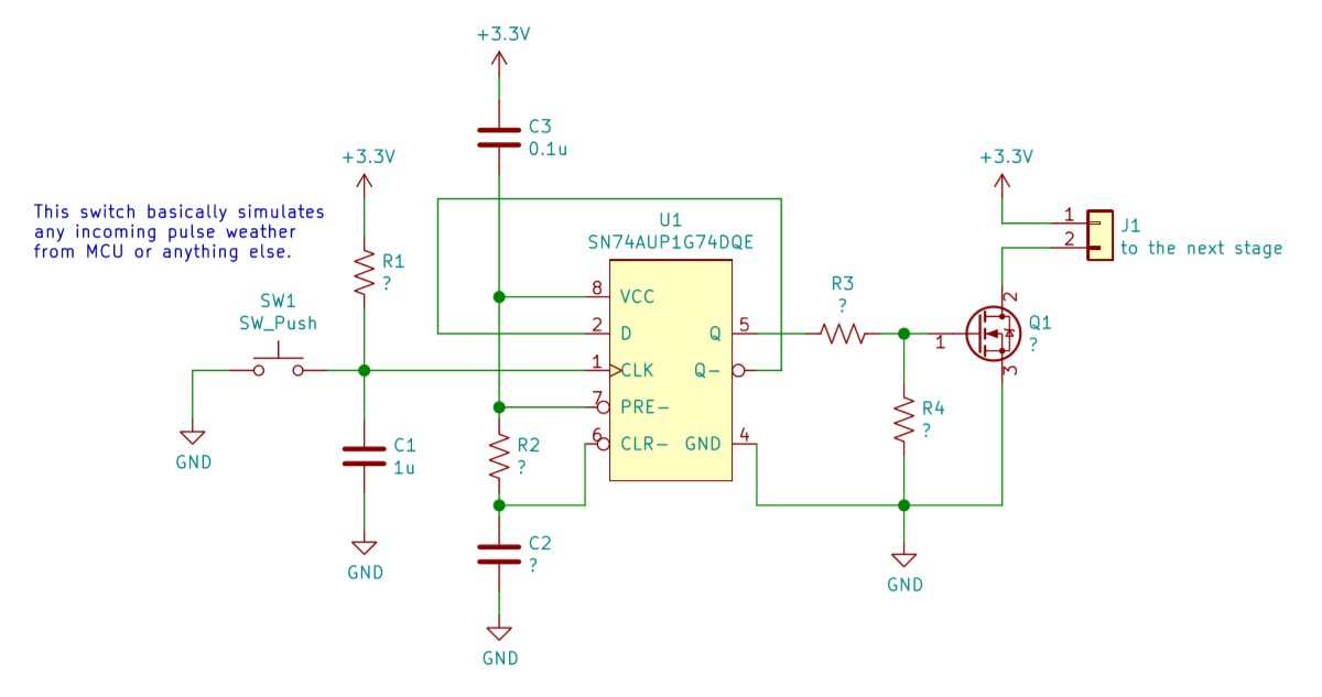
  • Here's what I came up with:

    This is basically partially a copy from SN74AUP1G74 typical power button circuit with MOSFET added as a switch.

    Well, I think with this schematic anytime "the button" is pressed (this could be any pulse, weather from an MCU or anything else) it will toggle the MOSFET switch on/off.

    Please let me know where I'm wrong as I'm doing this the first time.

    Also, I'm not sure yet how to calc resistors and capacitor values. But I'll try to read more about it.

  • Hm... I just noticed the SN74AUP1G74 typical power button circuit has the SN74AUP1G17 single Schmitt-trigger buffer. I believe I don't need it in case when the input is digital (like from MCU).

  • C3 is wrong; a decoupling capacitor most go between VCC and GND.

    R1/C1 would be needed only for debouncing a real button.

    R2/C2 results in a slow edge, so it might be advisable to add a Schmitt-trigger buffer. Size them so that you get a CLR pulse of the desired length.

    R3 is needed if Q1's gate capacitance is so large (> 70 pF) that the switching current would be too high. Size it so that the current stays below the absolute maximum rating.

    R4 is needed to keep the transistor off while U1 is powered down. It's typcially 100 kΩ.

    The pulse from the MCU will toggle the switch, but this has the risk that the state of the switch could go out of sync. A more robust solution would just connect PRE and CLR to the MCU.

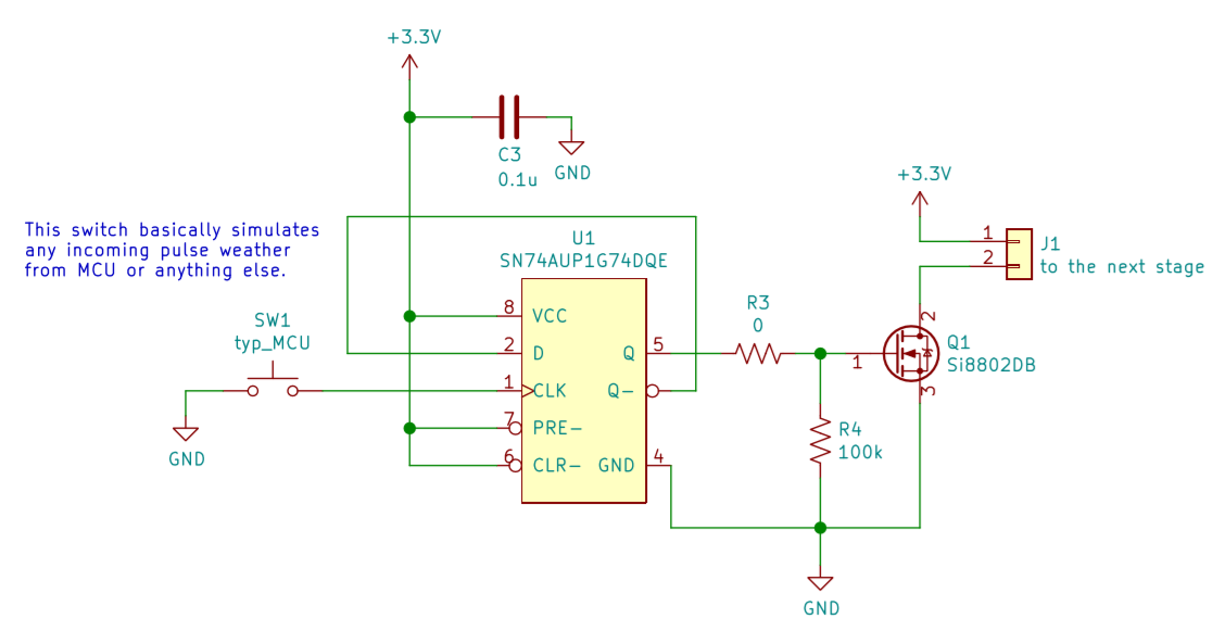
  • Yes, C3 is just a technical error.

    Removed R1/C1.

    I did not understand about R2/C2. The datasheet says:

    > The resistor and capacitor at the CLR pin are optional. If they are not used, the CLR pin must be connected directly to VCC to be inactive.

    Does this mean I can just remove them too?

    R4 - understood.

    I don't want to connect PRE and CLR to MCU as I might not have an MCU at all or I may not have free I/O pins available.

    MOSFET - I looked at some of them and I'm not sure I understand their datasheets fully. It looks like this one - Si8802DB - should be enough and I think I don't even need R3 at all. Also, soldering it with hot air might be a challenge. But I'd try it just to see how difficult it is.

    New schematic:

    Thanks again for helping me!

  • After powering up, R2/C2 delay the rising edge on CLR in order to bring the flip-flop into a known state. When both PRE and CLR are always high, then the initial state is unknown.

    That MOSFET isn't really meant for hand soldering. How much current do you need to switch?

  • ok, but when the circuit powers up the MCU is up and will set the state. Would this be enough if this happens within short period of time?

    Yes, I understand this MOSFET is not for hand soldering but I'm just curious if it's possible. So I'll try.

    The current to switch should be up to 500mA. I don't think I will need more.

    I'll try to add MCU to this circuit tomorrow. Just to have the whole picture.

  • In this circuit, the MCU cannot set the state, it can only toggle the state.

    I do not think that the Si8802DB is safe without R3. For 500 mA, it would be more appropriate to use a MOSFET with a smaller gate charge, such as the DMN2300U (or the DMN3200UFB4 or CSD17484F4 if you want a challenge).

  • I've just been reading MCU datasheet and changing the schematic accordingly. And this is not trivial at least at the moment...

    Let's get back to this one if you don't mind: "R2/C2 results in a slow edge, so it might be advisable to add a Schmitt-trigger buffer. Size them so that you get a CLR pulse of the desired length.". If understood that right I should either calculate the RC values (I believe this is an RC integrator) or to use Schmitt-trigger buffer ... which I have to read about more :) I'll need some time.

  • The result of the RC circuit is a slow edge; you probably need a Schmitt-trigger buffer to handle the slow edge.

  • Hi Alex,

    I can recommend using the SN74HCS74. It has built in schmitt trigger buffers. So you don't have to add these externally.

    Thanks!

    -Karan

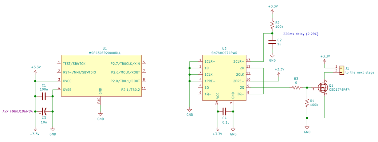
  • Karan, thank you for the suggestion as I was scratching my head here! ok, let me use this one instead of SN74AUP1G74. And I'll continue with the MCU then.

  • I've been creating a symbol for MSP430FR2000 and there's a note for pinout:

    > The ADC (signals A0 to A7, Veref+,and Veref-) is not available on the MSP430FR2000 device.

    For example, pin 13 is "P1.7/UCA0TXD/TB0.2/TDO/A7UCA0TXD/UCA0SIMO/VREF+". Does it mean this pin is NC and not used at all in MSP430FR2000? Or does it mean the pin is used for everything except A0 to A7, Veref+,and Veref- ?

    I'm confused. Here's the WIP:

  • I just realized that this is DC! Oops...

  • In table 4-1, the signals marked with footnote (7) are not available on the MSP430FR2000; this does not affect the other signals.

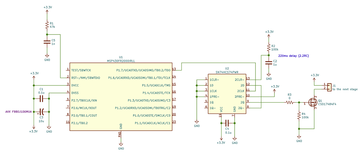
  • I was busy at work but here's the updated version:

    I put this according to MCU datasheet... Well, I think I haven't missed anything. Can you please look at this version and let me know if anything missing in here?

    Also, I noticed the Caution in the datasheet:

    > System-level ESD protection must be applied in compliance with the device-level ESD specification to prevent electrical overstress or disturbing of data or code memory.

    I have no idea what it means.

  • Looks OK.

    The built-in ESD protection is designed only for automated manufacturing. If any signal is connected to the outside world where a human can touch it, you need more ESD protection.

  • A-ha, again learnt something new.

    ok, let me create a PCB then!