This thread has been locked.

If you have a related question, please click the "Ask a related question" button in the top right corner. The newly created question will be automatically linked to this question.

LSF0108: application issue of LSF0108

Part Number: LSF0108
Other Parts Discussed in Thread: SN74AXC8T245

Hi, 

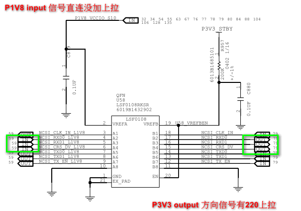
Customer uses LSF0108 with below schematic, the input signal  from P1V8 side(directly connected to the transmission chip without pull-up resistor) is output to P3V3 end via LSF0108( P3V3 side using 220ohm resistor), and found a low level  voltage 600mV; LSF0108 output signal is very poor when connecting to the terminal device(only 0ohm string resistance from SF0108 to terminal device); the signal has not significantly improved when trying to shorten the LSF0108 to the terminal chip distance; the signal is almost normal, except the 600mV low level offset when removing the terminal device.

Could you help to check what would cause this kind issue? How to improve the signal performance?

schematic:

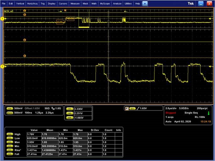
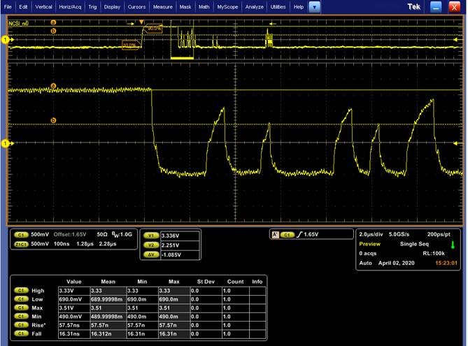
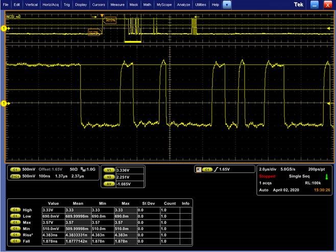
  test waveform:

1.  pull up resistor in RXD0 side is 220ohm

before level-shift(1.8V terminal )

after level shift(3.3V terminal), the high level is not rising to 3.3V.

removing the terminal device at 3.3V side.

Thanks.

  • The LSF is a passive switch. The 600 mV offset is caused by the output impedance of the 1.8 V device, which must sink the current flowing through the two pull-up resistors; on the 3.3 V side, add to that the voltage drop over the switch (which has about 10 Ω).

    The rounded rising edges are a typical sign of a high capacitance. This can be caused by long cables or connectors, but I do not know the input circuit of that terminal device.

    All signals are unidirectional, so it would be a better idea to use a direction-controlled level shifter with proper buffers, such as the SN74AXC8T245.

  • The input signal  of P1V8 side will has the same low level  voltage as the ouput signal of P3V3,

    1.When ouput signal pull up resistor is 220ohm, both sides have 600mv low level  voltage.

    2.When ouput signal pull up resistor is 10kohm, both sides have 50mv low level  voltage.

    Could you help to check what would cause this kind issue? Should I need to add pull up for P1V8 side?

  • The voltage is caused by the limited drive strength of the 1.8 V device.

    Adding a pull-up resistor would increase the current, and thus the voltage.

  • PCIe Smart NIC standard card using LSF0108 for NCSI,it will Communicate with host BMC device through cable.

    Based on my test results,found output pull up resistor effects the input offset voltage.

    Can I change the output (P3V3) side pull up resistor from 220ohm to 100ohm?

    It will cause higher offset voltage for this signal?

    It will cause damage to this IC?

    How much DB lose can this IC suffer?

  • Reducing the pull-up resistor value will increase the current, which will increase the offset voltage.

    The LSF is rated for up to 128 mA through the switch; 100 Ω would still be safe.

    If possible, use the SN74AXC8T245 instead.

  • Thank you for all your assistance.