This thread has been locked.

If you have a related question, please click the "Ask a related question" button in the top right corner. The newly created question will be automatically linked to this question.

SN74GTL2003: Product Selection

Part Number: SN74GTL2003
Other Parts Discussed in Thread: LSF0108, , TXS0102, LSF0204, TXB0108, TXS0108E, TXB0104, SN74LVC2T45, SN74AXC4T774, SN74LVC1T45

Hi Team,

Customer wanted to select one chip: 

  • Need to achieve interface voltage conversion, Such as iic, 7916 interface
  • Random conversion between 3.3V on one side and 1.62V-5.5V on the other

Customer thought that LSF0108/SN74GTL2003 has many constraints, such as differential pressure and the highest voltage only supports 5V.

Would you share you suggestion for this case?

Thanks,

Annie

  • Hi Annie,

    The LSF0108 lists the ROC spec as 5V, but it can support the typical 5V supply with +/-0.5V variation.

    In order to bypass the VrefB > Vrefa+ 0.8V restriction, I would suggest to have the VrefA at 1.65V supply and have the VrefB to 5.5V and pullup the IO ports to 3.3V / 1.65V / 5.5V as needed.

    The TXS0102 cannot support Vcca > Vccb in cases where the varying Vccb supply goes below 3.3V Vcca supply.

    GTL would also be similar in operation as LSF and would have the same restrictions.

  • Hi Shreyas,

    Thanks for your support. The customer has a few questions:

    Assume that the operating conditions of LSF0108 are: VrefA 0.95V VrefB is set to 5.5V, ioA side is fixed at 3.3V, B side is arbitrarily changed from 1.6-5.5V

    1. The IO port is pulled up to 1.65V-5.5V, is it any voltage on both sides of A and B, is there a limit of who is high and who is low?

    2. If the io pull-up on the A side is 3.3V, and the pull-up on the B side varies arbitrarily between 1.6-5.5V, can VrefB be less than 5.5V, such as 3.3V?

    3. VrefA and io pull-up & VrefB and io pull-up, are there any requirements for the power-up sequence when the chip is enabled? The customer needs the voltage on the A side to be fixed, and the voltage on the B side is constantly changing during the communication process.

    4. If the voltage on the B side is constantly changing from 1.6 to 5.5V, is it possible to fix the pull-up resistor to 310 ohms? Will it slow down the rising edge or affect the frequency at low voltage.

    5. Is it possible to share the simulation model of this device?

    6. Is there any better advantage of LSF0204? If customers want to use 4 io, can they replace each other?

    Thanks,

    Annie

  • Annie,

    we have great LSF application video collection done here which explains the basics of LSF translation, multi voltage translation, up and down translation among others. Please let me know if there are any questions on that.

    With VrefA at 0.95V, VrefB at 5.5V, you can pull up A and B ports to any value in between them. If you have the VrefB floating value such that it is b/w 1.65 and 5.5V, the A and B ports cannot exceed that VrefB value. So, case 2 cant be done.

    LSF0204 has integrated 200kohm biasing resistor as compared to the LSF010x series. Also, the output EN pin is slightly different as compared to LSF010x series.

    The simulation model for the LSf is in the PF below:

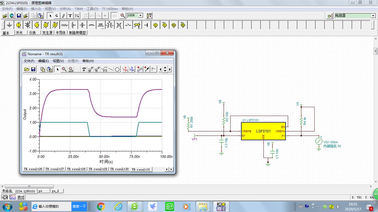
    A generic TINA model is attached here below:

    2234.LSF0101.TSC

  • Hi Shreyas,

    Customer has following question need your help.

    The customer copied the tina model you shared. If the pull-up resistor at terminal b is 310, the signal low level cannot be pulled down, but the manual recommends to pull up about 15mA. The customer would like to know if he is misunderstanding?

    Thanks,

    Annie

  • For pulling down to 0V, the driver must sink all the current through the LSF and yet maintain a low level. The LSF doesnt drive the signal to low level.

    PLease watch the LSF video series on the up and down translation as well as refer to the app note:

    The customer needs to have a weaker resistor ( like 1kohm) to bring down the Vol level in this case.

  • Hi Shreyas,

    The customer's selection needs are to achieve interface voltage conversion, such as iic, 7916, spi and other interfaces. One side is 3.3V. On the other side, any two-way conversion speed of 1.62V-5.5V level can reach 50M. Is this chip inappropriate?

    Can you help recommend a chip that meets the above requirements, or need to add a complete recommended solution for peripheral circuits based on a certain chip?

    The customer would like to know how the 100M rate is implemented in the lsf manual?

    Can TXB0108 solve this problem? Or other chips are suitable?

    Is TXS0108E OK? He wants to compare, can you share a tina simulation model?

    Thanks,

    Annie

  • Annie,

    The TXB or other buffered level translator is unable to handle the I2C signals which are open drain and bidirectional.

    The LSF is capable for 50Mbps support for both push pull and open drain signals, but have to work around the restriction of Vccb > Vcca + 0.8V.

    I could also suggest to consider using TXS0102 for I2C which wouldnt have high speed and using TXB0104 to support SPI and other push pull signals with 25Mhz speed.

  • Hi Shreyas,

    Is it possible to share tina simulation model of TXS0102 and TXB0104? Customer didn't find it on TI website.

    Another question is the spi needs to be 50M. May I know how to choose?

    Thanks,

    Annie

  • Hi Annie,

    we unfortunately do not have the tina spice simulation model of either of these devices.

    You can refer to the selection of level translators for various industry standard interface here below:

    For SPI, SN74AXC4T774 is suitable for 1.8 <>3.3V translation. but for higher levels, you would need SN74LVC2T45 ,SN74LVC1T45 devices.