Hi,
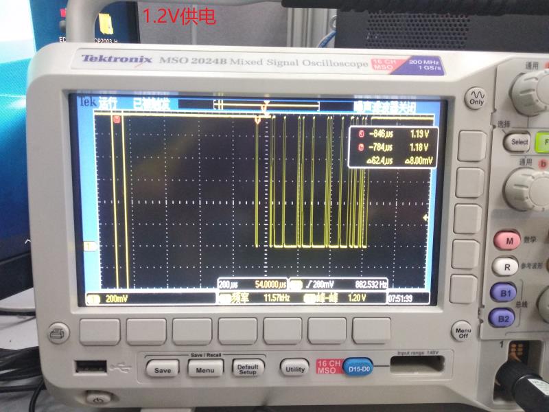
Please find the application block diagram as below. Figure 2 shows the 3.3V signal at B port and figure 3 shows the signal at A port.
Question:
The signal at A port is not as expected and signal at A port could be improved by lowing down the VCCA to 1.2V. Does the OE pin necessarily need to be pulled down? What's the possible cause for the phenomena? Thanks.