This thread has been locked.

If you have a related question, please click the "Ask a related question" button in the top right corner. The newly created question will be automatically linked to this question.

CD74ACT297: PLL circuit implementation

Part Number: CD74ACT297
Other Parts Discussed in Thread: SN74LV4046A, , SN74LV393A

I'm trying to wrap my head around the usage of the aforementioned integrated circuit. I'm aware of how a PLL generally works but as the datasheet of this IC is the only source of information I have, I'm a bit lost how to integrate it into my circuit.

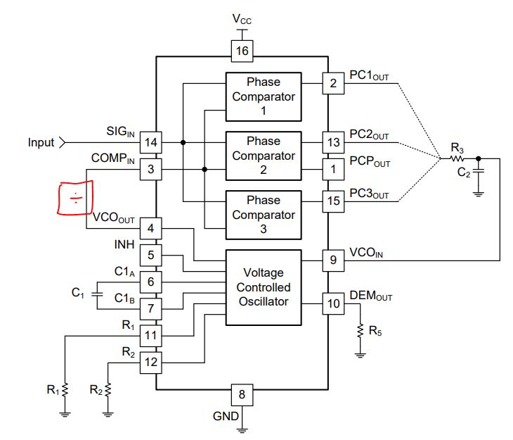
I need the PLL to generate a frequency that is 256 times higher than the input frequency which is a clean 50% square wave at around 80kHz - so, the output frequency is at ~20.5 MHz . The frequency division is taken care of using a counter IC. As I understand PLLs in general, the input signal (80kHz) must be applied to φA1, the output of the frequency divider is fed back to φB and the input to the divider is my output frequency (at 20.5MHz), when the PLL is locked. Input φB is also at 80kHz in this case.

But this digital PLL has a lot more pins that have to be some kind of filter and a controllable oscillator in a form that isn't obvious to me. Where does that leave the Mfc input and the I/D in/out, the modulo controls and so on? What frequencies are we talking about on those inputs and outputs for my usage scenario? The datasheet seems to have math as an answer to that question but I'm certainly not a math type of guy so some kind of usage instructions or even an example schematic diagram would be very helpful. Does it need more external components than the frequency divider?

Thanks!

Thomas

  • Hi Thomas,

    I think the trouble you're running into is that this device doesn't include an oscillator.  Basically it just has a counter and 2 types of phase detectors (XOR and Edge Detect) packaged together, and you'd have to provide an external VCO.

    I would recommend looking at the SN74LV4046A -- this is a more all-inclusive device and there's a ton of material out there on the '4046 function and how to use it ('LV4046 works the same as 'HC4046).

    Without going into too much detail on the design, you basically pick 2 resistors (R1, R2) that set your center frequency and frequency offset, then connect one of the phase comparators to a low-pass filter (usually an RC) and loop back to the VCO_IN pin.  For your application you also need a frequency divider (counter) between pins 4 and 3, indicated here:

    I would recommend sticking with PC1, which is an XOR based comparator, if possible. As long as you have a square wave with ~50% duty cycle, that should work well for you. The other PCs can be a bit finicky.

  • Hi Emrys,

    thanks for the quick reply. I must have read through the '297 datasheet a dozen times and I still haven't found anything about the absence of an oscillator. Actually, quite the contrary. This is from the second sentence in the description, for example:

    This device contains all the necessary circuits, with the exception of the divide-by-N counter, to build first-order phase-locked loops as shown in Figure 1.

    If the datasheet ever gets a new revision, it might be a good idea to include that information...

    Anyway. When looking for parts, I've also come across the SN74LV4046A as probably suitable but eventually decided to go with the CD74ACT297. I guess I'll give it another try, then.

    Thanks!

    Thomas

  • Hey Thomas,

    I completely agree.

    When I first read the datasheet it sounded like there was an oscillator, and it took me a bit to figure out that there wasn't one. It was quite odd that it didn't include any mention of an external oscillator -- especially with the statement you quoted.

    We're currently overhauling the old HC family datasheets, but when we get to these I'll be sure to improve the clarity so others don't run into the same issues. I've added this information to our errata tracker so we won't forget about it later.

  • Hi Emrys,

    I'm glad to hear that you consider to improve the datasheets.

    In the meantime I have (actually quite accidentally) found an old TI application note from 1997 that discusses circuit applications for an IC from the same family or a predecessor of the CD74ACT297. The math in there is still way over my head but it somewhat paints a clearer picture ;)

    I have ordered the PLL IC you mentioned earlier and see how that turns out.

    Thanks again.

    -Thomas

  • For your application (80 kHz input, 20.48 MHz output, assuming 5V supply), I would recommend starting with these values for the '4046:

    R1 = 3.5 kohm

    R2 = open

    C1 = 43pF

    Let me know if you run into any trouble - I'm always around to help.

  • That's awesome, thanks!

    Do these values for R1/R2/C1 target the VCO's output frequency (20.48MHz) or the much lower input frequency of the PLL?

  • They are for the VCO configuration (20.48 MHz) -- although they are not exactly for 20.48MHz center frequency:

    Basically I was recommending to set it up to provide the maximum speed that it can, and then counting on the loop to reduce the frequency to 20.48 MHz exactly and lock.

    You might have to tweak the resistor value a bit (maybe increase to 4.7k or 10k), but most likely it will work directly with these settings.

    Do you know what counter you'll use for the 'divide by 256' circuit yet?

    I'm thinking that the SN74LV393A would be a good pick since it has 2x 4-bit counters in one package that you can easily configure into an 8-bit counter. Since it's in the same logic family, you can expect similar performance & a good match to the PLL.

  • Yes, I have a 393 counter for this purpose on the bench. At the moment, it's not a TI one, though... ;)