This thread has been locked.

If you have a related question, please click the "Ask a related question" button in the top right corner. The newly created question will be automatically linked to this question.

LSF0108: clarify pull-up requirement for low (A) side in DOWN translation

Part Number: LSF0108


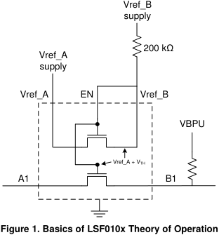
I would like to clarify exactly how DOWN translation operates and what the need for the pull-up is on the lower voltage side.  In my example I have a bi-directional 3.3V logic CMOS gate with a separate direction pin and I am translating that to an FPGA pin operating in a 1.8V bank.  VrefB and EN is tired to 3.3V through 200k.  VrefA is tied to 1.8V. 

When the B side gate is driving a logic high, near 3V, my understanding is that the internal 4-terminal FET will be ON as long as the B side voltage is less than 1.8V.  This makes the A side follow the b side up to 1.8V.  Then when the B side signal crosses 1.8V, the FET turns OFF.  If a pull-up is connected on the A side o 1.8V, this will allow current to be supplied to the FPGA input from 1.8V after the FET is OFF.

Is my understanding correct so far?

The data sheet and application video state the pull-up to 1.8V is optional provided the A side gate is not leaky.  But if the signal is in a steady state high,  and NO pull-up on the 1.8V side (A side) is included, then does this design count on the input capacitance to hold the level at 1.8V?  IS this reason why the input can be too leaky?  It seems like a conservaoive design would include pull-ups and not count on receiver input capacitance to hold the charge.

Please clarify my understanding.

Thank you

Craig

  • The reference transistor circuit regulates the gate voltage so that a small current (limited by the 200 kΩ resistor) flows through the FET.

    The gates of all other FETs also are at the threshold voltage above Vref_A; this means that a small current could flow if A1 is at Vref_A. However, the gate is already at the threshold voltage, so that current stop flowing when the A1 voltage begins to go higher than Vref_A.

    The A1 voltage cannot go lower without a load that is able to sink the current.

    The currents involved are very small, so you can easily pick up noise. TI says that "pullups to Vref_A are not required but allow heavier loads on the
    low side and help with signal integrity issues that may arise." And there is no guidance for predicting whether signal integrity issues actually will arise.

  • I am still not clear on the clamping mechanism on the A side.  The data sheet Table 2 states that for B to A down translation with B = High, the "A-side is clamped at ref_A (2).  Note 2 states that the A-side can have a pull-up to Vref_A for additional current drive capability or can even be pulled up to a higher rail than Vref_A.

    My confusion is in the area of the clamping action.  If the FET turns OFF when the signal on B is equal to Vref_A how is the A side drain (or source) clamped?  It seemed to be that the design is counting on a small capacitance to hold the charge when the lower FET shown above turns OFF?

    I must be dense but I am not seeing how the clamping works.

    Craig

  • Hey Craig,

    I'd recommend checking these training videos out on the LSF family. They should help address your concerns.

  • There is no clamping. Nothing prevents the voltage at A1 from going higher than Vref_A (which is why pulling it up to a higher voltage works).

    But without a pull-up resistor, there is nothing that actually tries to make the voltage go higher.