This thread has been locked.

If you have a related question, please click the "Ask a related question" button in the top right corner. The newly created question will be automatically linked to this question.

LSF0108: what is the recommended R value with variable VCCB?

Part Number: LSF0108
Other Parts Discussed in Thread: SN74AXC8T245, SN74LVC8T245

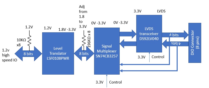
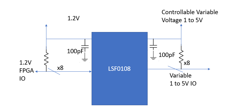
1)      A circuit is needed to accept any kind of logic between 1V to 5V (we will vary the pull-up voltage accordingly) and interface to an 1.2V IO, I proposed this one, any proposal for the value of the resistors? Consider highest rate up to 400 MHz if possible …

i look at the level shifter selection guide.

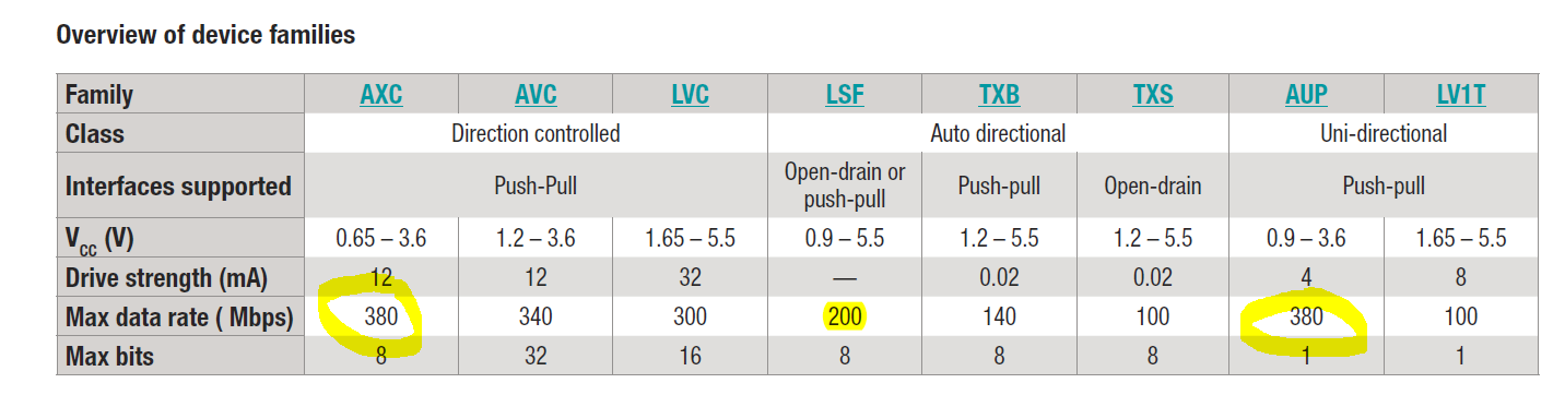
it seem to me, the max data rate for LSF family is only 200Mbps. Am I right to say the closest family that i should used are Direction controlled/uni-directional level shifter as circle above AXC or AUP family. Any recommendation for the proposal for the value of the resistors?

Best regards,

KPK

  • The LSF datasheet makes suggestions for the pull-up resistors. But the achievable speed depends also on the capacitances of your board, so you have to measure the waveforms. And it's possible that the FPGA or the external device do not have enough drive strength for the resulting current.

    The AXC and AUP families do not go above 3.3 V, and the highest speed is achieved only at the highest supply voltage.

  • Hey KPK,

    That frequency is too high for any of our level translators. This requirement will be difficult to meet, but the LSF family may be the best fit. Here are some training videos covering the LSF family (covers how to select resistor sizes):

    https://training.ti.com/node/1139264

  • hi Dylan,

    Can you suggest the optimum value of the resistors for variable values 1V to 5V? or how can we find the optimum value of the pull up resistor? 

    Best Rgds,

    kpk

  • Hey Kpk,

    Video 6 in the series I linked in the last post will cover pull-up sizing (up translation video). It will provide you with design considerations as well.

  • Dear Dylan,

    Will you be able to confirm if the following connection is alright? Any additional considerations or things to correct.

     i wish to have a hardware interface that let us have LVDS, but also other voltage formats of up to 3.3V in this case specifically. Please, see Fig.1, there it is shown that we foresee to have 8 I/O pins, so this 8 pins would be used to support bidirectional LVDS format (for this I use the LVDS transceiver DS92LV040ATLQA/NOPB) but if I want to use other format voltage other than LVDS this would be also possible (logic levels of up to 3.3V) and for this it is used the multiplexer block which selects between signals of LVDS transceiver  or signals directly from I/O pins. Then, it is considered a level translator (LSF0108PWR) which let me have the signals at the proper level.

    Best rgds,

    kpk

  • Are there always four transmit channels and four receive channels? Because in that case, you can simply replace the LSF with a SN74AXC8T245.

  • but the AXC and AUP families do not go above 3.3 V, and the highest speed is achieved only at the highest supply voltage. Am I right?

  • Your last statement was that voltages go up to 3.3 V. I do not know what voltage you actually need; this is something you have to decide yourself. If you want 5 V, use the SN74LVC8T245.

    (Please note that the AXC can do at least 250 Mbps at 1.8 V, which is still better than the LSF.)