This thread has been locked.

If you have a related question, please click the "Ask a related question" button in the top right corner. The newly created question will be automatically linked to this question.

TXB0108: Circuit with two TXB0108 connected in series

Part Number: TXB0108
Other Parts Discussed in Thread: SN74AXC8T245

Dear TI Team

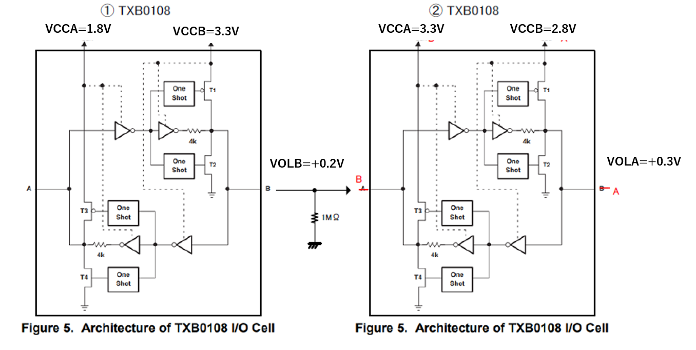
I would like to ask about TXB0108.

Our customer is considering a circuit in which two TXB0108 are connected in series as described above.

When the output of the CPU connected to A on the device side of ① is set to Low, VOLB = +0.2V and VOLA = +0.3V in the above figure.
However, when the output of CPU was set to Low with the device of ② removed, VOLB=0V.
We would like to set VOLB=VOLA=0V due to the above circuit specifications.

I think that the value of VOLB became +0.2V and VOLA=0.3V due to the effect of the output current flowing through the 1MΩ pull-down resistor between the devices of ① and ②.

Although not shown in the data sheet, is it necessary to have a 1MΩ pull-down resistor between ① and ② for the above connection?
(By the way, the data sheet says that the pull-down resistor used outside the TXB0108 output must be 50 kΩ or more.)

  • Hello,

    This type of configuration with this device is not recommended. 

    Due to the nature of the device where it has weak output drivers on all I/Os there could be bus contention between the weak driver on the VCCB side of the first device and the VCCA driver on the second device.

    When Device 1 tries to drive the line high with a 4kOhm output impedance and Device 2 is in a low state, it could settle at 1/2*VCC, which is not a good situation.

    The reason why the pull down resistor must be large is because the output drivers are weak, and if it is small it will not be able to overdrive the pulldown when switching.

    I would not recommend this configuration, and i would encourage you to use either:

    1. A single TXB to do 1.8 to 2.8V translation directly (no reason to have 3.3V in between unless you have separate boards/cards/modules, in which case i would not recommend the TXB device in the first place because it does not tolerate large capacitive loads well (cabling, connectors, other physical interfaces to another board)).

    2. SN74AXC8T245 as an 8-bit buffered dual supply translator so that you have appropriate drive strength to drive a capacitive load if necessary.

    Best,
    Michael

  • Dear Michael

    Thank you for your reply.

    I would like to ask adding following questions.

    1.After checking the data sheet, the following specifications of VOL were described. Is the specification of ① in this case the same as the following specifications?

    2. Is it correct to recognize that it is possible to use the two SN74AXC8T245 that you have suggested, under the above conditions?

    (Of course, this is based on the assumption that DIR is set.)

    Regards,

    Y.Ottey

  • Hey Ottey,

    I'm not exactly sure what you mean by the first question, but yes those would be the Vol conditions on the A port of device 1 since its connected to a CMOS input.

    Two of the SN74AXC8T245 can be used in series since its a buffered device (As long as the directionality is set correctly to avoid bus contention)

  • Hi Dylan

    Thank you for your reply.

    I explained to our customers that we do not recommend using the TXB0108 in series as described above.

    After that, our customer decided to change the voltage conversion from 1.8V to 2.8V using one TXB0108.

    However, they received a request to find out why VOLB = +0.2V when the output of device ① is low when the above TXB0108 is connected in series.

    After checking the following materials, I saw that VOL changes as shown in the following equation when a pull-up resistor is attached to the data line.

    https://www.ti.com/lit/an/scea043/scea043.pdf?ts=1598406517833

    From this, the following phenomena are inferred:
    ・When devices (1) and (2) are connected in series, the pull-up resistor (Rpu=60kΩ) is connected to the output due to the internal resistance of device (2), and VOLB becomes about +0.2V.
    ・When the device ② is removed, the pull-up resistance disappears, resulting in VOLB=0V.

    Do you agree with the above recognition?

    Regards,

    Y.Ottey

  • Hey Ottey,

    That's a good way to look at it, essentially the additional TXB device adds a load current of ~55 uA which causes that voltage offset across the internal 4k resistor. This would be equivalent to a 60kΩ pull-up to 3.3 V.