This thread has been locked.

If you have a related question, please click the "Ask a related question" button in the top right corner. The newly created question will be automatically linked to this question.

CD74HC7046A: CD74HC7046A

Part Number: CD74HC7046A

Hello
I used R1-270K, R2-220K, C1-100PF to get 500KHZ, I want to lock the frequency to the mains (50HZ).
I did a frequency division and I used PC2.
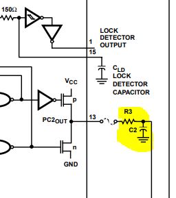
Can you help me calculate LPF values?
(R3, R4, C2).
Best Regard
Itamar

  • Hi Itamar,

    For the simplest low pass filter, you only need 2 components:

    There are essentially two factors in calculating this:

    (1) Time required to stabilize the output

    (2) Output voltage ripple

    Ideally, the filter would take zero time to update the output to the correct voltage, and that voltage would be a perfect DC value.  Of course, this isn't really possible. You can spend a long time with the math trying to optimize both of those items, but I find that to be a waste of time for a first order filter.

    I usually recommend choosing a low pass filter corner frequency of ~ 2 orders of magnitude less than the desired operating frequency.  In this case, the corner frequency would be at 0.5 Hz.

    The formula for the corner frequency of a first order low pass RC filter is: f_c = 1/(2*pi*R*C)

    So, we can rearrange that formula:

    R*C = 1/(2*pi*f_c) = 1/pi = 0.3183

    To get close to that value, we need pretty big R and C values.  I'd start with a 1uF capacitor, since those are extremely common and easy to get.

    R*(1e-6) = 0.3183

    R = 0.3183e6 = 318.3 kohm

    Selecting the nearest 1% resistor value gives 324 kohm.

    So, the final first order low pass filter design would be

    R3 = 324 kohm

    C2 = 1 uF

    Going back to our 2 criteria, note that this will settle in ~5RC = 1.62 s, which is a relatively long time for a circuit.

    The output voltage ripple will be ~76 mV at 5V input, which I would consider to be very good.

  • Hi

    Thanks a lot for the information it's much clearer now.
    Unfortunately I used values according to the calculation, I get the desired frequency 500khz but I do not have a lock on the 50hz.
    I tried testing with a potentiometer without any noticeable improvement.
    Is there a solution to the problem?
    What is the stability of the VCO?
    I attached pictures of the signals (the file name is according to the pin number).

    (pin-1, pin-13 , pin-4 )

    Best Regard

    Itamar     attached pictures of the signals (the file name is according to the pin number)

  • Hi Itamar,

    It looks like the output of the VCO is exactly what we'd expect (500 kHz). Can you show the two inputs to the phase comparator? 

    Also, that last image of the VCO output looks quite odd - like there's an issue with the ground of the device or probe. It should be reaching ~0V on every cycle. I would recommend double checking all ground connections and make sure you have a decoupling capacitor. If that all checks out, you might try another unit to see if this one has been damaged.

  • Hi Emrys

    Indeed, I get 500KHZ but I would expect the PV2-OUT will be in high impedence and the Ld will be in constant high level.
    I used decoupling capacitors in all the components.
    The problem with VCO output was because the scope.
    I attached the two inputs you requested.
    Of course the Comp_in is at 50HZ.
    Thank you very much for your help.

    Best Regard

    Itamar

  • When you take scope shots of logic signals, they generally need to be on the same display (2 channel or more) -- unless you're just looking at signal integrity. Otherwise you can't see the related timing and the data isn't very helpful. I can understand that we don't all have 8 channel scopes, but it's extremely hard to troubleshoot a logic circuit if you can't see the inputs/outputs on the same display with the same time scale.

    From my experience, I've found that the PC2 comparator is the most prone to errors and can get into a state where it's 'stuck' changing between hi-z and either high or low depending on the timing of the signal inputs.

    It looks like your circuit is doing what it's supposed to though - the signal is ~50 Hz. If you can view the COMP_IN, SIG_IN and PC2_OUT signals on the same scope shot, you can follow the logic diagram in the datasheet and figure out what's going on.

  • I apologize for my late response I was on a weekend break.
    I attached the two inputs: COMP_IN, SIG_IN.
    I did not attached the PC2_OUT because the measurement affects the signal. Logically the circuit works fine .I expected the difference between the phases to be zero and this is not the case, even though I get the desired frequency

  • What happens when you connect the PC2 output to the scope? I wouldn't expect much change for that node with a high-impedance scope probe.

  • I attached two pictures of the measurement of the signals.
    The first with Prob X10 and the second with Fet Prob (Referring to the photo in the previous email)
    You can see that there is an effect of the probe, also you can see that the circuit logic works correctly

  • The 10x mode of the scope probe adds a 9 Mohm resistor in series with the internal 1 Mohm resistance of the scope, so you can expect some variation in the signal with that.

    It looks like the PC2 comparator is doing what it's supposed to do - it is high impedance at the start of the plot, allowing the voltage to hold at ~2V (from the capacitor), then forces the output high to charge the capacitor a bit, and finally releases the line again, leaving the capacitor at about 2V.

    I think you're seeing fluctuations in the phase due to the slow response time of the loop filter.

    It's possible to add an active loop filter to do this, but that's beyond the range of support I can provide.

  • I understood . Thanks for all the help