This thread has been locked.

If you have a related question, please click the "Ask a related question" button in the top right corner. The newly created question will be automatically linked to this question.

SN74LVT16244B: Difference between AVC and LVT

Part Number: SN74LVT16244B

Hello team,

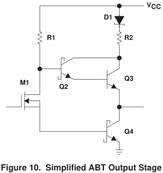
I have a question on the basic structure of LVT family regarding the ICC, IC's supply current. I checked AVC(Advanced Very-Low-Voltage CMOS) is based on CMOS logic and LVT (Low-Voltage BiCMOS Technology) is based on BiCMOS(TTL+CMOS) logic.

I can see ICC is different depending on output status as attached. For AVC family, ICC is same regardless of output status. What's the difference between CMOS family and this BiCMOS family that cause this ICC difference?

Thank you for your kind answer.

  • ABT Advanced BiCMOS Technology Characterization Information says:

    Figure 10 shows a simplified schematic of an ABT output stage. Data is transmitted to the gate of M1, which acts as a simple current switch. When M1 is turned on, current flows through R1 and M1 to the base of Q4, turning it on and driving the output low. At the same time, the base of Q2 is pulled low, thus turning off the upper output. For a low-to-high transition, the gate of M1 must be driven low, turning M1 off. Current through R1 charges the base of Q2, pulling it high and turning on the Darlington pair, consisting of Q2 and Q3. Meanwhile, with its supply of base drive cut off, Q4 turns off, and the output switches from low to high. R2 is used to limit output current in the high state, and D1 is a blocking diode used to prevent reverse current flow in specific power-down applications.

    The higher supply current of ABT devices is needed as base current for the bipolar transistors (Q2/Q3/Q4).

    That the ICC value for high outputs is so low is a measurement artifact: the base current of Q2/Q3 flows not out of the GND pin but out of the output pin and into the load, so it is not included in ICC.