This thread has been locked.

If you have a related question, please click the "Ask a related question" button in the top right corner. The newly created question will be automatically linked to this question.

CD4050B: CD4050B

Part Number: CD4050B
Other Parts Discussed in Thread: CD4098B, , CD4013B
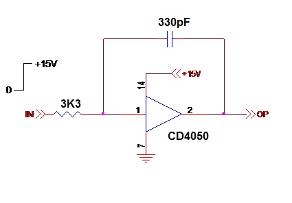
Hello

I wish to use the following Ckt for a Min Pulse width creation for our Three Level Inverter.

Four such Ckts shall be used per leg. Approx 800 nS to 1.1 uS is the target Pulse Width 

for both On & Off.

PS is +15V and Input Signals too are 0-15V.

I have the following queries:

1. At the Negative Transition point, the Input would be momentarily pulled below Gnd

  where the internal Clamping Diode shall reset the 330 pF cap thru the Rdson of the O/P Stage.

  Is the Internal clamping diode ( to Gnd ) good to take this repetitively?

2. At the Positive Transition point the Input shall go above the +15V.

  Would it be destructive for repeated pulses?

3. If I choose to incorporate a Series Diode at the Input, either end to +15 & Gnd

   but do not insert a limitaing Resistor with the 330 pF Capacitor, would that be okay?

Thanks and regards

Varun

  • The image is as shown below-

  • The absolute maximum rating of the internal clamping diodes is 10 mA. Your circuit will exceed this.

    Adding external Schottky diodes would help.

    Would it be possible to use the CD4098B instead?

  • Hi Varun,

    I would recommend against using the below circuit. The expected switching voltage is VCC/2, which would be 7.5V across the diode.

    When switching from low to high, the input voltage will be forced to 22.5V, which can immediately destroy the input gates of the CD4050B.

    When switching from high to low, the input voltage will be forced to -7.5V, which will likely destroy the input diode due to over-current (it's only rated to 10mA).

    Also - it appears that the circuit won't produce pulses at the output, just a replication of the input with a slight delay & added voltage/current spikes.

    I would recommend to use an XOR based edge detector instead - delaying one input slightly will produce a positive output pulse at every input edge, both positive and negative. An XNOR can be used for negative pulses instead.

  • Many Thanks to Clemens and Emrys for your prompt replies.

    While much of what both of you say is valid for many applications,

    in my specific case they aren't.

    It's actually a variant of our Short Pulse Suppression Ckt where I need some 

    4 Nos per Leg on my Three-Level Inverter Driver.


    My target specs are as follows:

    Input Pulse Train: fsw Max as 10 kHz.

    Pulses shorter than 900 nS +/- 200 nS are to be killed, for both Positive as well as Neg Pulses.

    Equivalent Delay at the Rising & Falling edges, though not reqd, is tolerable.

    Ckt to be operable @ +15 V ( Alas, that limits the options !! )

    Four such Ckts together, Footprint & Package count does matter.

    Coming to Clemens's reply, If I put Schottky Diode Pair at the Input, clamped to PS rails,

    do I additionally need to put a resistor in series with the Cap, in case the O/P Stage of CD4050 requires?

    Thanks and regards

    Varun

  • To add on to my prev mail.

    A simple R-C Ckt with a Schmitt Trigger why that I don't prefer?

    Normally that meets the Specs, but has this issue:

    When say Rising, when Vth+ is crossed, O/P Toggles, and the 

    Input immdly starts falling.

    In that case, the Time is determined by ( Vth+ - Vth- only ) while normally 

    it is from Vcc to Vth- for falling & 0 to Vth+ for rising.

    In that case for a guaranteed Min Short Pulse, the spread of that SPS time

    becomes unacceptably large.

    This Ckt obviates that problem, hence preferred.

    Regards

    Varun

  • For a deglitch circuit, you need a multivibrator (½ CD4098B) and a D-type flip flop (½ CD4013B). Connect the input signal to both trigger inputs (+TR and −TR) of the multivibrator and to the data input (D) of the flip flop. Connect the inverted output (Q) of the multivibrator to the clock input (C) of the flip flop. Tie the multivibrator's RESET input high and the flip flop's SET and RESET inputs low. Configure the multivibrator's R×C for 900 ns.

    Any edge in the input signal will trigger (or re-trigger) the multivibrator. This means that its Q output goes low and stays low until the configured time has elapsed without any new edge on the input.

    When Q goes high and triggers the clock of the flip flop, the new, stable state of the input is copied to the flip flop's Q output. (After a glitch, the new state is the same as the old state.)

  • Hi Clemens

    An excellent Ckt and has been used by me before.

    If I had just one ( or two Ckts ) would be ideal; however

    here I need four such & will require 2 X CD4098 & 2 X CD4013.

    If my ckt can be tweaked, one package of CD4050 may suffice.

    Coming to my initial Ckt:

    If I clamp the Input with Dual Schottky Diodes, clamped to PS Rails

    ( to protect the internal Clamp Diodes ) do I additionally need to put

    a Resistor in series with the Capacitor, to protect the O/P Stage?

    If so, what may be the Min value of that Resistor?

    Thanks for your very prompt response.

    With best regards

    Varun

  • There is no absolute maximum rating for the output current.

    Use RθJA to derive the maximum power dissipation, and check that against the actual power dissipation (VOL × IOL or VOH × IOH per channel). Size the resistor so that the current is low enough.

  • Hi Clemens

    Many thanks for your answer.

    If I don't put any external Resistor, only the internal Rdson 

    would come into play which if I read the Data Sheets correctly are:

    Rdson ( H ) 4.5V / 15 ma = 300E Worst Case

    Rdson ( L ) 2V / 32 mA =  62.5E Worst Case.

    The Energy dissipated in those Rdson shall be 1/2 C*V^2 at every edge; or

    E = Fsw X C*V^2 which @ 10 kHz  & 330 pF which works out as 0.74 mW

    Four such gates would be 3 mW total.

    With Rth j-A as 81.2*C/W for D ( SOIC ) package the Delta T is minuscule.

    Would you be kind enough to have a cursory look at my calculation to check

    if I have not made any egregious mistake.

    Thanks and regards

    Varun

  • You should not calculate the total energy over time, because the power dissipation must be limited at any point of time.

    If we allow a temperature offset of +25 °C, the maximum power dissipation is about 300 mW, or 75 mW per channel.

    At the moment when the output has just switched, the capacitor pretty much shorts the output to ±15 V (minus the diode drop). Figures 6-3…6-6 do not show the maximum current (where the power dissipation would be highest), but we can see that the current at 15 V would be much too high.

    If you add a 1.5 kΩ resistor in front of the input to reduce the diode current to less than 10 mA, the output current also is less than 10 mA, which is safe even in the worst case.