Because of the holidays, TI E2E™ design support forum responses will be delayed from Dec. 25 through Jan. 2. Thank you for your patience.

This thread has been locked.

If you have a related question, please click the "Ask a related question" button in the top right corner. The newly created question will be automatically linked to this question.

SN74LVC2G125: Noisy clock output from one of Buffers inside the Chip

Part Number: SN74LVC2G125

Hello,

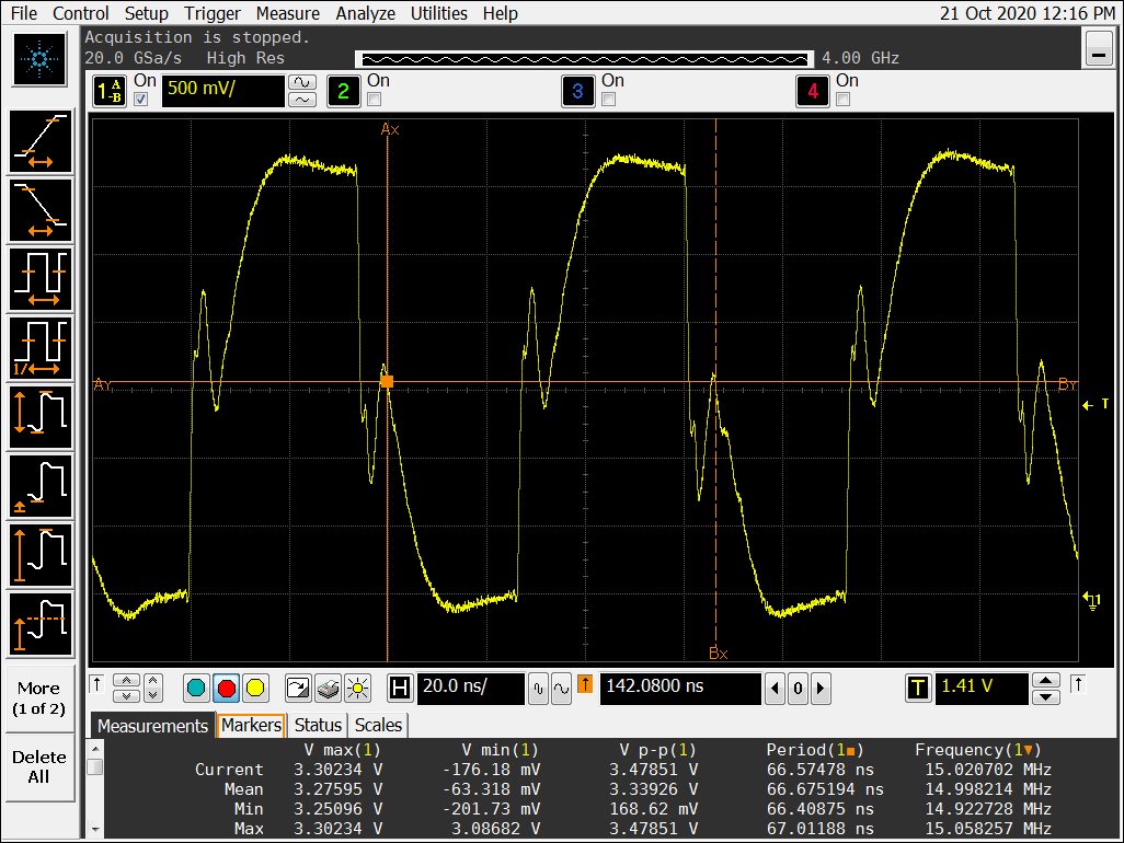
I am having signal integrity issues in one of the Buffer outputs. I`d like to understand what could be causing it ? Some incorrect implementation? Do the 2 buffers inside the chip work differently?
Attached the schematics and Buf(2) images. The same was observed t 3 different samples.
I assumed it could be an impedance mismatch and changed the series resistance R1405 to 0, 22, 27, 30, 33, 46 and 75ohm, but it did not solve the problem.


Thanks,

Jhonathan

  • Hi Jhonathan,

    Both buffers work the same in the device, and they are very simple internally.

    This looks like reflections from the transmission lines used. It's most likely due to the layout.

    It's odd to see two damping resistors on a single output (R1403 and R1404) -- there should really just be one physically close to the output if required.