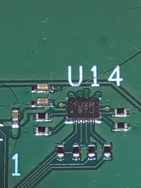
We designed a board where we are using the B-side as inputs and A-side as outputs. However we see 1.177V at the B-side. Can you help check to see if this is correct?
This thread has been locked.
If you have a related question, please click the "Ask a related question" button in the top right corner. The newly created question will be automatically linked to this question.
We designed a board where we are using the B-side as inputs and A-side as outputs. However we see 1.177V at the B-side. Can you help check to see if this is correct?
Here is some additional information:
Regardless whether OE_N is high or low, I still see the same measurements. Seems like 1.177V for one board, another board shows 1.212V.
The JTAG_xxx signals are hooked up to a JTAG connector, with a 100k pull-up to 3.3V, which is not being driven. All measurements on A-side or B-side are done on floating nets.
1. If VCCA is powered down to 0-300mV and VCCB is 3.3V, B-side shows 1.2V, A-side shows 0V.
2. If VCCA is powered on to 1.8V and VCCB is 3.3V, B-side shows 1.2V, A-side shows 0V.
3. If VCCA is powered on to 1.8V and VCCB is 0V, B-side shows 1.2V, A-side shows 0V.
The strange part is the ~1.2V from the B-side. I am expecting 3.3V because of the pull-ups I have on here.
Part
Footprint
I will update more as I get more status.
If you want the lines to be pulled down.
If the lines need to be pulled up, you need stronger pull-up resistors.
Hey Phillip,
I would recommend 10 kohm pull-ups if possible. However my concern is with the fact that this issue is apparent whether or not the I/Os are disabled. When the I/Os are disabled you should not have this issue with the glitch suppression circuitry acting as a weak pull down.
Let me know if you are able to retest with 10 Kohm and if it fixes the issue.