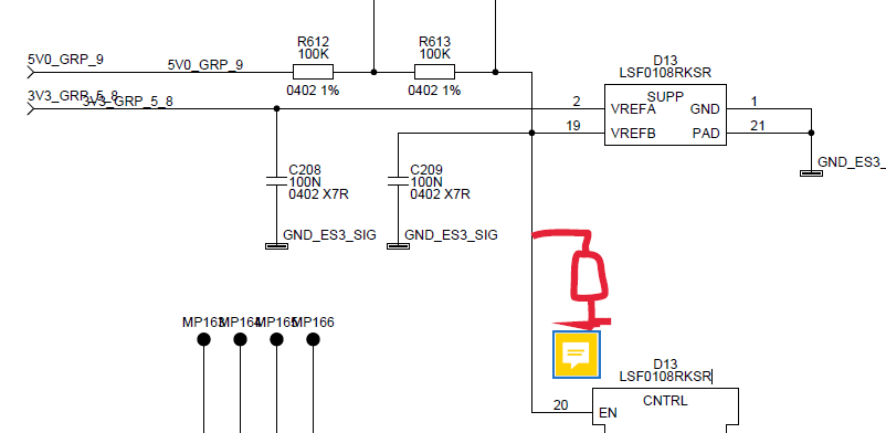
Part Number: LSF0108
Good morning,
I am using LSF0108 chips in my design mainly for receiving 5V signals and converting it to 3V3.
I did the schematic entry based on the datasheet info. VREFB is 5V and VREFA is 3.3 and 200 ohm resistors are connected to VREB input and enable signal.
My question here is, 3V3 is enabled first and 5V is enabled after 3V3. Before the chip is enabled VREFA is applied to component.
I couldn't find anything opposed to this in data sheet but I wanted to make sure if this approach is true.
I attached the screenshot from my circuitry
Best Regards