This thread has been locked.

If you have a related question, please click the "Ask a related question" button in the top right corner. The newly created question will be automatically linked to this question.

LSF0102: Debug LSF0102 for 3.3V to 1.24V

Part Number: LSF0102
Other Parts Discussed in Thread: SN74AUP1G34, PCA9306,

Hi,

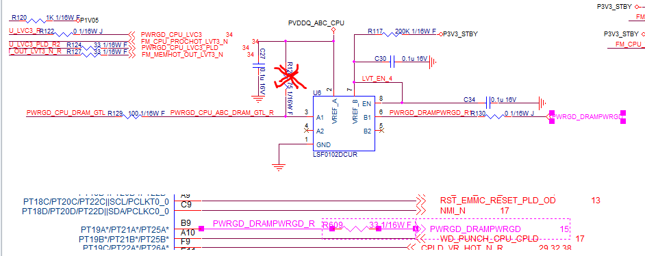
Will you help to take a look schematic below. Customer approve to post question and waveform to e2e.

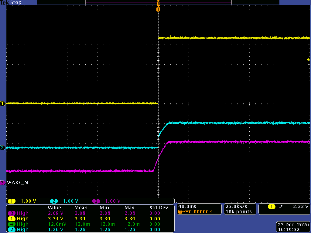
Question :Why A1 is measured with 1.4V while AVref is connect to 1.23V?

Application:

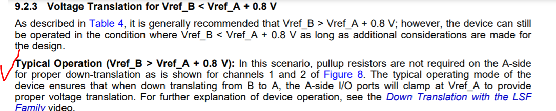
1.Down convert 3.3V to 1.23V from B side to A side. The Bvref is connect to  3.3V, and Aref is connect to 1.23V.

2.Push pull connection.

3.The pull up resister R128 is removed with the scope waveform show as below(showing A1 is measure ~1.4V which is not our expected 1.23V.)

  • C30 and C34 are in parallel; this is not necessary.

    A small current flows into Vref_B and out of Vref_A. If the PVDDQ_ABC_CPU supply is not able to sink this current, then the supply will float up. To work around this, add a resistor between PVDDQ_ABC_CPU and GND.

    Alternatively, connect the LSF differently: leave Vref_A and Vref_B open, and connect EN directly to PVDDQ_ABC_CPU. (This always requires the pullup on A1.)

    Alternatively, for unidirectional downtranslation, use a buffer with an overvoltage-tolerant input, such as the SN74AUP1G34.

  • Clemens Ladisch said:

    C30 and C34 are in parallel; this is not necessary.

    A small current flows into Vref_B and out of Vref_A. If the PVDDQ_ABC_CPU supply is not able to sink this current, then the supply will float up. To work around this, add a resistor between PVDDQ_ABC_CPU and GND.

    Do you have suggest value to for resistor?

    Alternatively, connect the LSF differently: leave Vref_A and Vref_B open, and connect EN directly to PVDDQ_ABC_CPU. (This always requires the pullup on A1.)

    Alternatively, for unidirectional downtranslation, use a buffer with an overvoltage-tolerant input, such as the SN74AUP1G34.

  • A safe estimate for the leakage current is (3.3 V − 1.23 V) / 200 kΩ ≈ 10 µA. (The actual current will be smaller because Vref_B is somewhat above Vref_A.)

    So the resistor should be at most 1.23 V / 10 µA = 123 kΩ. Just use 100 kΩ.

  • Clemens Ladisch said:
    A small current flows into Vref_B and out of Vref_A. If the PVDDQ_ABC_CPU supply is not able to sink this current, then the supply will float up. To work around this, add a resistor between PVDDQ_ABC_CPU and GND.

    We found from statement form datasheet, and think we connect follow this instruction. Should the datasheet need to be change?

  • That statements talks about the I/O signals. The resistor I've proposed is needed on the power supply. (See section 8.1.7 of the PCA9306 datasheet.)

  • Hi Clemens,

    This is FAE Vincent, I have suggested customer to add a 100Kohm resistor between PVDDQ_ABC_CPU and GND per your recommendation, but it didn't work.

    You can find the waveform below, the PVDDQ_ABC_CPU is still raised to 1.44V. Should using a lower resistance one instead, or do you have any advice?

    Besides, you also suggest a alternative solution "leave Vref_A and Vref_B open, and connect EN directly to PVDDQ_ABC_CPU. (This always requires the pullup on A1.)", does it mean not to supply voltage on both Vref_A and Vref_B but only to power EN pin with PVDDQ_ABC_CPU? Do we need to pullup on B side as well?

    Thanks a lot.

    Vincent Chen

  • In theory, 100 k should be enough. Is it possible that the 1.44 V comes from somewhere else?

    A pullup on the B side is needed if the B side is an output, or if the B side is an input coming from an open-drain output.

  • Hey Vincent,

    Sorry for the partial post before - I accidentally sent that before I was done editing.

    I noticed that the output of the LSF has a mostly linear appearance:

    This isn't a typical RC charge curve. It looks to me like there's a constant current slowly charging the input, which could be leakage through the LSF device.  Typically this small amount of leakage current sinks into the receiving device, but if it has an extremely high input impedance, the current can theoretically drift up like this.

    The simplified explanation of how the LSF works says that the channel MOSFET turns off when it's in the high state. This isn't entirely true - the MOSFET is mostly off when the output is clamped as shown (no pull-up resistor), but it still provides a small amount of current to keep the output at the specified voltage. Most CMOS inputs have a small amount of leakage. which will set the output voltage. In this case, it looks like the small amount of leakage current is charging the input of the receiving device very slowly (it takes 28ms, which is quite a long time in logic-world).

    To give you some numbers, the charge rate shown above is approximately (1V / 28ms = ) 35.71 V/s.

    Assuming a 5pF load (which probably isn't far off), then the amount of leakage current we're talking about is (5pF * 35.71V/s = ) 178.6 pA.

    They could try putting a large pull-down resistor at the output of the LSF device to see if this fixes the issue -- between 100kohm and 1 Mohm should be sufficient to sink the leakage current.

  • Hi Emrys, Clemens,

    Thanks a lot for your support. Now customer solved issue by adding 100kohm pulldown resistor at output pin(A1 pin). Here is the waveform. (CH1 : B1, CH2 : A1, CH3 : EN)

    There are few items need your advice.

    1. The correct solution is adding 100Kohm pull-down resistor on A1 pin, remove C30 and no need of pull-down resistor on Vref_A, correct?

    2. Ven equals to Vref_A + Vth, is it correct? If this is a case, what is the Vth of LSF0102?

    3. In the waveform below(CH1 : EN, CH2 : Vref_B, CH3 : Vref_A), the Vref_B(3.3V) is supplied first and you can find there is a voltage about 0.66V that is established at EN pin. Is it normal and why? 

    Could it be the threshold voltage?

    Thanks very much.

    Vincent Chen

  • Hi Vincent,

    It looks like the 1.23V supply is still charging in the first waveform shown:

    (1) above shows that the bias voltage starts to increase before the voltage transition. The only cause I know of for this would be an increase at VrefA. I'm sure if they probe that supply together, they will see that the waveforms match.

    (2) above shows that the LSF device starts to conduct when the bias voltage reaches a specific value, which is the threshold voltage. If they measure the bias voltage and the input voltage at that point, the difference between them will be approximately the threshold voltage. In other words, V_GS = V_G - V_S

    (3) above shows that the output waveform follows the bias voltage, as expected.

    In the second waveform, if your VrefA = 0V, then your bias voltage will be VrefA + Vth from the diode connected nFET. Yes, it's expected. The video here explains how this circuit works: https://training.ti.com/tlm-lsf-bias?context=1134826-1139264-1134790