


Other Parts Discussed in Thread: SN74LVC2T45, SN74LVC2G17
Hi team,
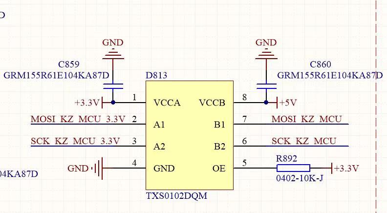
My customer is testing TXS0102. The schematic is as below. B1 B2 are input pins and they are from a 5V MCU. A1 A2 are output pins to a 3.3V MCU. And B2—>A2 is a clk signal of the SPI interface, B1—>A1 is a data signal of the SPI interface .
We measured the signal on A1 and A2 pins as below. CH1=A1 Pin=Data signal. CH2=A2 pin=CLK signal. We found the data signal is not stable during high level.

Then we disconnect the CLK signal from 5V MCU to B2 pin and only let Data signal go through from B1—>A1. Then we measured the output data signal on A1 as below. The data signal becomes stable during high level.
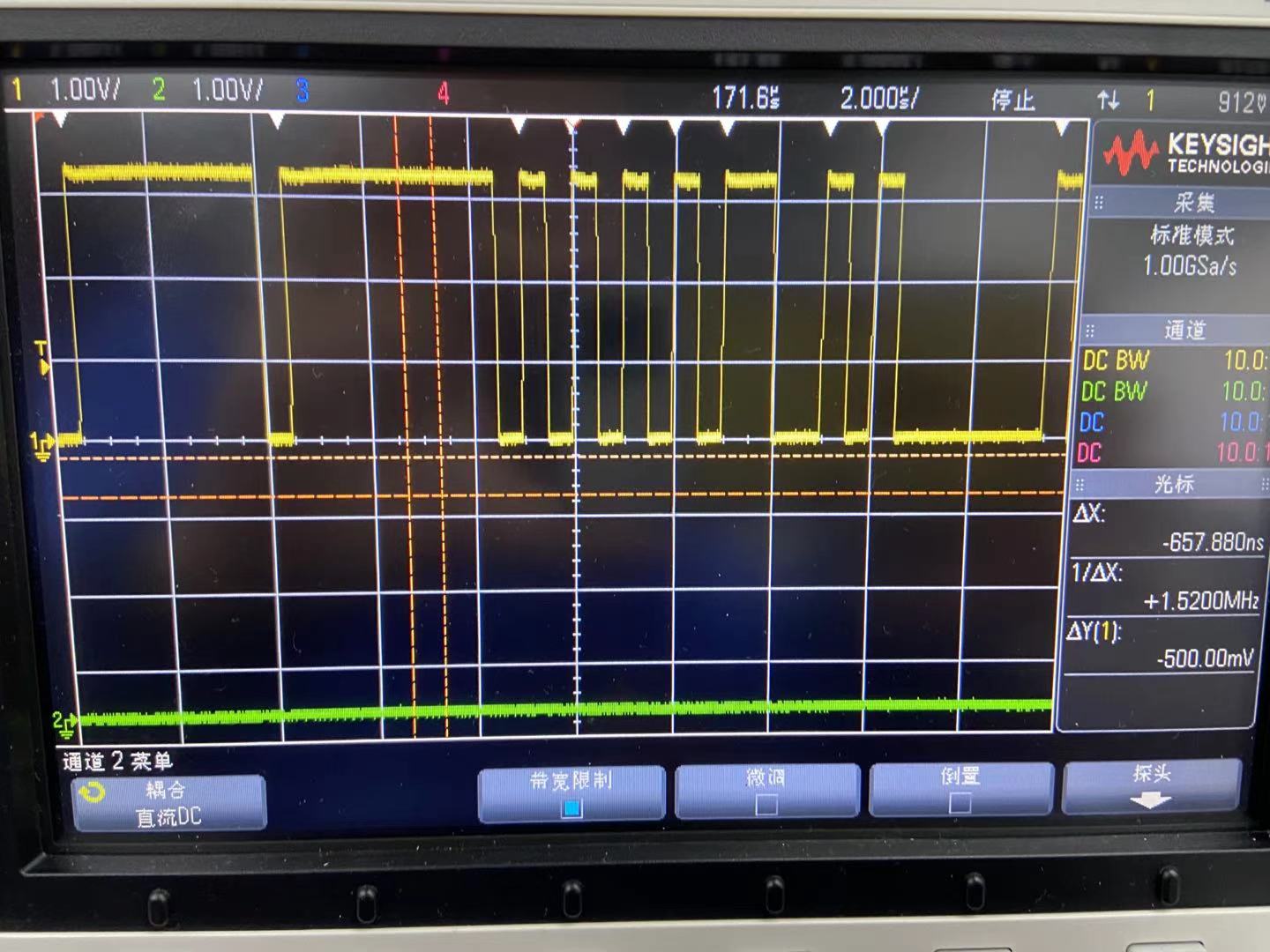
So based on the above tests, it seems the clk signal through TXS0102 has a bad effect on its adjacent data signal. So do you have any advice on why this happens? Thanks.
By the way, the 3.3V and 5V power supply are both from LDO which is very stable.
Best regards,
Wayne

