This thread has been locked.

If you have a related question, please click the "Ask a related question" button in the top right corner. The newly created question will be automatically linked to this question.

TXB0304: High leakage current on TXB0304 when VCCB is off during system sleep mode while VCCA always ON.

Part Number: TXB0304

Dear Sir/Madam,

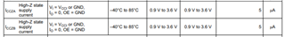
Please help to confirm with TI TXB0304 datasheet of the Ioff below as per spec table below.

Does it means the leakage current? 

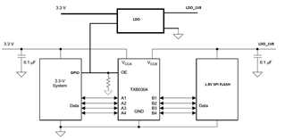
With application circuit below, the highlighted red above in the table is it correct leakage current for our case?

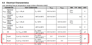
And for highlighted red above, A port mean for 1 port leakage or total A ports leakage?

Which leakage is suitable for our case from the spec if above highlighted leakage is not for our application circuit? Main reason for asking, we have the send the part for FA and the result is NO fault found. 

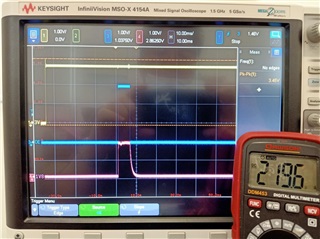
We have having 50% rejected rate due to high leakage current during off mode. The VCCA always supplied but VCCB is off during system sleep mode. And we can seen the high leakage current in our product. Can you advice any issue with this connection?

Best regards,
Felix


  • What is the state of all the pins, especially Ax, in off mode? Are they floating?

  • Hi..

    Thanks for the response.

    There are in high impedance state from the MCU, and I did the pulled down externally on the Ax pin but the leakage still there.

    Beside this Ax pin, what other will cause this high leakage on VCCA when OE and VCCB is Off?

    Regards,

    twg

  • Hi.

    For the TI leakage current table snapshot above,

    Could you advise that the Ioff for A port is belong to 1 port or all the A ports leakage?

    Thanks,

    Regards,

    twg

  • The specification is per pin.

    Can you determine whether the current flows into VCC, into OE, or into some I/O pin?

  • Hi.. 

    So the leakage of 1uA at 25C need to multiply by 4, become 4uA,  correct? 

    Do you know what is typical leakage of Ioff? 

    Confirmed leakage is to VCC pin. 

  • I did cut the trace of 3V to VCCA,  and the leakage current become normal and replace new level shifter,  the leakage current become normal too .

  • Total have 6 pins,  VCC,  OE and 4 IO,  so the max leakage is 6uA,  correct? 

    Please confirm 

  • Hi Wee,

    What is the exact leakage current you are measuring? Each I/O will have its own leakage as well as the control inputs. Vcc leakage is essentially Icc.

  • Hi.. 

    We are measuring the ICC current and found that the result of current leakage from 20uA to 1000uA which do not meet the spec limit of ICC current .Any idea why ICC have so high leakage current? 

    From the Ioff spec table above,  the max leakage 1uA is per pin for the A port,  this per pin is for IO? From the spec,  where is ICC leakage for the Ioff case? 

  • Hi Wee,

    I can't really say for sure with the limited info provided. It is recommended to power down both supplies at the same time in the Power Supply Recommendation section which is likely to avoid a state such as this. You didn't say or not the state of your OE pin, is this being driven to a valid Logic state (specifically Low)?

    Right below the Icc spec:

  • Hi.. 

    Yes..Our OE is driven low and VCCB is low. We do have external PD resistor on OE pin. 

    For our case,  VCCA always powered,  OE = low,  and VCCB is 0V. From your spec stated in Ioff there,  the supply can be switch off either VCCA or VCCB = 0V as stated snapshot extracted from the spec. Am I interpret correctly? 

  • Hey Wee,

    Yes, you are interpreting the spec correctly. The top row is for the VccA = 0 V case and the bottom row is for the VccB = 0 V case.

    Do you have a current probe compatible with an oscilloscope? This would be useful to see how the current reacts during the whole power down process.

  • Hi Dylan,

    Please see the attached picture.

    Setup condition:

    3V to VCCA

    OE with PD resistor of 100KR

    1.8V to VCCB.

    3V, OE and 1V8 probed at scope and 3V connect in series with a multi-meter to the VCCA. you can see that the result of 3V always powered, OE and 1V8 is always low but the leakage is ~220uA. We have confirmed that root cause is come from the TXB0304. 

    Let me know why the ICC got so high leakage current when OE and VCCB is low.

    Can you help to ask your FA team to check with this condition for the 3x failures units that we have sent to her?

    Because her first FA report cannot duplicate the issue.

    Thanks,

  • Hi Dylan,

    We want to tabulate out the total leakage current for the production to follow the limit, but we need to know the leakage when VCCA powered, OE and 1V8 is low, may I know what is the max leakage current for my case? Can we follow Ioff leakage current of 1uA/port as per you said that the specification is for a port.

    From my understanding, this Ioff is for total leakage current on ICC when only one side is powered, am I correct interpreting?

    Appreciate if you could advise.

  • Hi Dylan,

    For level shifter leakage current, can I put the leakage current as per table below.

    We want to tabulate the leakage for production to follow the limit of leakage.

    Typ
    ( uA )
    Max
    ( uA )
    Level Shifter
    Ioff ( 4 Ax pins) 8
    OE to GND 2
    3V to VCCA 5
    GND to VCCB 5
  • Hi Wee,

    I wasn't involved in the FA process and not sure who you are referring to, but typically the process involves a lot of testing to determine if there is damage to the device. This seems to be a specific state of the device with the configuration you have it in which is likely why no issues were found during the process.

    Is this 220 uA present until VCCA is powered off or until VCCB is powered back on?

    As for the table, I would remove the last row since the supply for VccB I assume won't be supplying any current when powered off.

  • The lady is from Shanghai, China and her name is Tricia,  Is there possible help to inform for the test again. 

    The 220uA leakage current will goes to off when VCCA powered is off.

    Mobile phone offnoted of the table. 

  • Hi Dylan,

    As you said that It is recommended to power down both supplies at the same time in the Power Supply Recommendation section but it also mentioned that TXB0304 has circuitry that disables all input/output ports when either VCC is switched off (VCCA/B = 0 V), that mean this IC still able to powered either VCCA/B only, so TI FA team have carry out this test condition in your test case?

  • Hi..

    Can we leave the Ax port floating to TXB0304 Ax ports?

    Is there any issue?

  • Hey Wee,

    Its recommended to power both rails down due to there being a potential floating node internal to the device causing a slight supply increase. This is likely why powering off VCCA fixes the issue as well. Powering down one of the supplies will disable the I/O, but there's also a potential supply current increase from not powering down both supplies. Due to the architecture of this translator, its ok to leave the A port floating.

  • Hi Dylan,

    In order to prevent the leakage current when VCCA powered and OE and VCCB =0 and TXB0304 is in high impedance state.

    What state should we set on A1 - A4 ports from the processor ?

    Because both side are in high impedance state during operation mode.

    Is there an issue?

  • Hi Dylan,

    We can't re-spin the design to disable both VCC powered because this board already in production

    We must know the way to eliminate this high leakage current from software setting if possible.

    Appreciate if you could help to answer the previous question that I asked.

    we want to know what state setting for A1- A4 is suitable from the host if TXB0304 is in high impedance state.

  • Hi Wee,

    For the I/O its best to keep them at GND. This can be done by adding weak pull-downs to the I/O, I recommend 100 Kohm or more to avoid contending with the internal resistor.

  • Hi Dylan,

    With our high leakage current case, we can have 2 ways to resolve it.

    1) Terminate the VCCA

    2) Powered 1.8V to VCCB when OE is ground.

    Can you tell me why there is a leakage with our case of powered VCCA, and OE and VCCB is ground?

    and we did connected A1 - A4 ports to our MCU and set them to high impedance port and input pull down.

    Do you know what is the logic/mechanism in this IC internally?

    Because it cannot duplicate this issue in your FA test and our failure rate was 30~40%

  • Hi Wee,

    I didn't perform the testing so I'm not going know to what you are referencing for the FA test. As for the high current draw you are seeing, this is likely due to you powering down the VCCB while leaving the VCCA supplied. This can lead to a potential internal float which would result in high supply current. The way to avoid this is to power down both supplies as recommended in the data sheet. The impact of the internal float will vary over process.