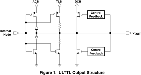
I ran a simulation in HyperLynx 2.8 with the IBIS model for this device, and got very strange results. I also looked at the similar 74AUC34 (without hysteresis on inputs) and see the same thing. The pullup and pulldown curves have significant discontinuities in the switching region, and the '34 file mentions that this is due to "feedback circuit". This does not make sense as the '34 does not have hysteresis, and in any case it should not cause that effect. In addition, the rising waveform has a slope reversal in the curve near the peak (between 1.8V and 2.2V on the V=0 curve) which I have never seen before. The falling waveform has a similar, although less pronounced, inflection point at around 250mV. I believe this gives me the slope reversal in the simulation waveform (attached) which is most pronounced in slow/weak PVT corner. Note, this is the 2.5V Vdd curves, AUC34_OUT_25 and AUC17_OUT_25 which are essentially identical.
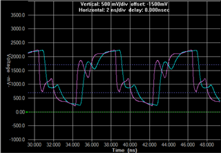
Are these IBIS waveform anomalies just an artifact of the IBIS file, and can be edited out; or do these really reflect the behavior of the part? I would like to use it to buffer an RGMII interface, running at 125MHz, but I am concerned about double-clocking due to the strong non-monotonic waveform shown (light blue trace is the receiver at the die, the pale purple trace is the waveform at the 17/34 driver die).
Is there another part that I should be looking at instead? Requirement is for six channels, non-inverting, at 2.5V Vdd. Operating temperature is -40C to +85C. Output to output skew must be low, <100pS.
Thanks.