


Hi Dear,
I have a question about my project listed below.
It is need to design level shifter between FPGA and DUT. The DUT will be I2C device. Voltage level (Vccb) from FPGA is set to 3.3V, but from DUT side must be regulated between 1.65V to 5.3V. This is need to make some test with DUT.
For this I made schematic (fig.1) using 2 independent level shifters (TXB0102- U1, U2) to cover the specification of the TXB0102 – Vcca < Vccb; 1.65V< Vccb< 5.5V; 1.2V< Vcca< 3.6V and voltage of the second shifter need to adjusted 1.65V to 5.3V.
Is it possible this schematics work properly. If NO – why.
Thanks for advance.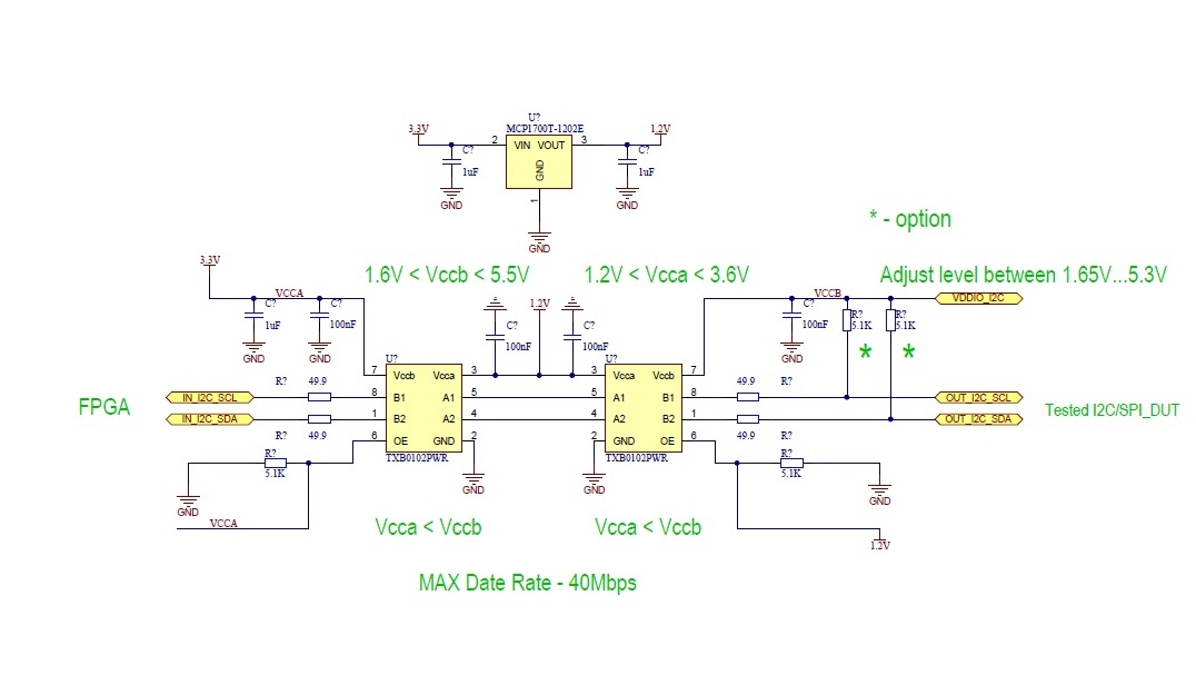
fig.1

