This thread has been locked.

If you have a related question, please click the "Ask a related question" button in the top right corner. The newly created question will be automatically linked to this question.

SN74LV4046A: SN74LV4046A

Part Number: SN74LV4046A
Other Parts Discussed in Thread: CD74HC4046A

Hi team

Now i use it as only phase comparator ( meaning i don't use its VCO).on my apprication, there is another Vcxo on the circit.Then,how will PCout act when i put the Ccxo clock.Then,how will PCout act when i put the same Vcxo clock to each of SIGin and Comp_in?

in other words,The Vcxo controlled by this IC and the Vcxo making the reference clock are in the same state, on my apprication.

Thank you very much.

  • Hello,

    This device has three separate phase comparators (PC1, PC2, PC3). The behavior of each is explained on page 11 of the datasheet, copied here:

    This device is designed to very closely match the CD74HC4046A, which has a fairly detailed block diagram of the internal workings. Copied here:

    When a signal is applied to SIG_IN and a clock is applied to COMP_IN, all three phase comparators are active simultaneously. Typically, the output from only one is required.

    If the input signals are both square waves with 50% duty cycle, I would recommend to use PC1 as it is the most reliable and simplest. SIG_IN and COMP_IN will be frequency matched, but at a 90 degree phase difference by design.

    If the input signals are not 50% duty cycle, one of the other two PCs must be used.

    PC2 will match the phase of the signals as well as the frequency. PC2 uses a 3-state output approach based on an internal counter. A higher frequency at SIG_IN will cause the output to be driven 'high' and a higher frequency at COMP_IN will cause the output to be driven low. In between these states the output will be in high impedance.

    PC3 operates similarly to PC2, however it uses a 2-state output, only going between 'high' and 'low' outputs. This is a more reliable system, but also uses more power.

  • Thank you for help.

    Now i use only PC2 becouse i need PLL locking voltage in the range of 0.3~3.0V.

    I consider like attached curcit design.

    When the VCOX that makes the reference clock signal (that is put to COMPin)  and one that is controlled by this IC, i guess it may be never locked.

    Becouse the reference freaquency made by VCOX will be faster(or slower) when the SIG that is also made by the same VCOX will be faster(or slower).

    How do you think about this?

    it can be locked or not?

    4705.PLL curcit.pptx


  • First one comment - I would recommend to connect pin 5 (INH) to VCC to disable the oscillator and prevent additional power consumption/noise while you use the phase comparators.

    If the inputs have significantly different frequencies, that should be ideal for PC2 to work -- it operates based on how many rising edges it 'sees,' so a large difference in frequency helps it to quickly enter a state that will correct the frequency difference.

  • Dear Emrys-san

    Thank you for helping me.

    I'll connect INH to VCC and check whether signal made by PC2 changes. 

    BR,
    Taku Kato

  • Hello Kato-san,

    I think I may have misunderstood - I thought you had not yet built this circuit.  Are you saying that this circuit is already built and is not working properly?

    If so, can you share oscilloscope shots of the input and output signals? Pins 3 (COMP_IN), 13 (PC2_OUT), and 14 (SIG_IN) should be sufficient.

  • Hello

    thank you for your reply.

    I have already built this circuit.

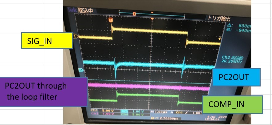
    It is not working well when i use 'LRCK' signal as one goes to COMP_IN.

    I send you the signal image.

    BR,
    Taku Kato

  • Hello Kato-san,

    It looks like COMP_IN and SIG_IN both are getting multiple triggers due to ringing on each clock edge, which is likely what is causing issues. Since this is an edge-triggered phase comparator, each edge will change the state of the output and can cause it to fail to lock.

    It also looks like there is a great deal of noise in this system, which also could be a factor.

    It also appears that SIG_IN and COMP_IN are exceeding the device's absolute maximum rating for input voltage (Vcc + 0.5V)

    You could attempt to clean the signal with an RC filter at the input - I would start with values of 22 ohms and 22 pF to prevent slowing the signal edges too much while still providing some ringing reduction.

  • Dear Ermrys-san

    Thank you for your reply.

    i set INH Hi, and use snubber circuit, it works well.

    thank you for helping me.

    BR,
    Kato Taku