Other Parts Discussed in Thread: SN74CBTLV3861-Q1, SN74HC151
Dear, Sir.
My customer's P.C.B was completed, after then they are facing a neceesity of modification.
The voltage on input line is changed to 5V, output is 3.3V which is connected to MCU.
The power supply is providing 3.3V for SN74HC151-Q1 VCC, too.
The best way would be put LDO, Voltage translator, etc, but there is no space for such modification.
They are considering more simple way as ;
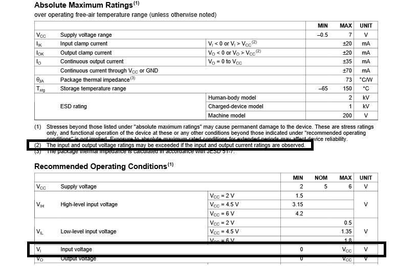
SN74HC151-Q1 has the internal power clamp diode on input, so the series resistors will be put on input
pins to limit the input current.
I believe the real input pins voltage would be 3.3V(VCC) + Vclamp(diode VF), even if almost of voltage
will be dropped at the series resistors.
I would like to get your advice on followings ;
1. Is it no problem to realize 5V input capability taking above simple way?
2. On the datasheet, VI MAX(Input volatge MAX) is limitted on VCC.
Can the nromal operation be expected under 3.3V(VCC) + Vclamp(diode VF)?
Best Regards,
H. Sakai