This thread has been locked.
If you have a related question, please click the "Ask a related question" button in the top right corner. The newly created question will be automatically linked to this question.
Dear, Sir.
My customer's P.C.B was completed, after then they are facing a neceesity of modification.
The voltage on input line is changed to 5V, output is 3.3V which is connected to MCU.
The power supply is providing 3.3V for SN74HC151-Q1 VCC, too.
The best way would be put LDO, Voltage translator, etc, but there is no space for such modification.
They are considering more simple way as ;
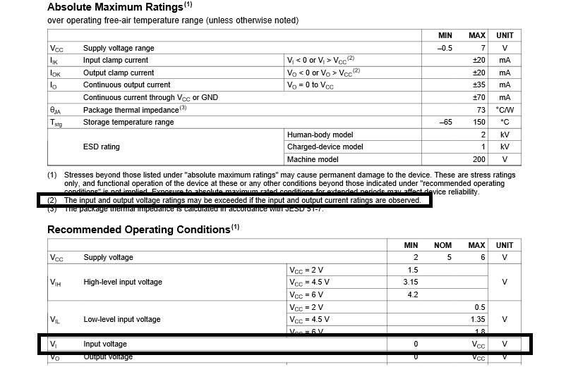
SN74HC151-Q1 has the internal power clamp diode on input, so the series resistors will be put on input
pins to limit the input current.
I believe the real input pins voltage would be 3.3V(VCC) + Vclamp(diode VF), even if almost of voltage
will be dropped at the series resistors.
I would like to get your advice on followings ;
1. Is it no problem to realize 5V input capability taking above simple way?
2. On the datasheet, VI MAX(Input volatge MAX) is limitted on VCC.
Can the nromal operation be expected under 3.3V(VCC) + Vclamp(diode VF)?
Best Regards,
H. Sakai
Hi Sakai and Emrys,
There is an idea just came across. Please allow me to go through a question list.
Your requirements are
1. automotive qualified
2. 8:1 multiplexer
3. input signal is 5V and output is 3.3V. voltage translation is required
Here are my solutions:
Solution 1. using SN74CBTLV3861-Q1 (10 channel 1:1 switch) to do voltage translation and then SN74HC151-Q1 (8:1 MUX)
Here is the way how to use SN74CBTLV3861-Q1 to do 5V to 3.3V translation.
Solution 2: If the customer thinks the above self-biasing circuitry is too complex, they may use SN74CB3T16210-Q1 + SN74HC151-Q1. This is TI's integrated solution. It's 20 channel. Unfortunately, we don't have 8 channel version for automotive. Here is how to use it. Very simple.
Solution 3: I am not sure if the customer can use SN74CBTLV3861-Q1 or SN74CB3T16210-Q1 without SN74HC151-Q1. It depends if the customer really needs signal driving capability and inverting output.
The voltage translating switches I am talking about do not have signal buffering/repeating capability, while SN74HC151 does. In addition, SN74HC151 has an inverting output, W pin, that voltage translating switches do not have.
Dear, Wang-san and Emrys-san.
I am feeling a mount of gratitude for your valuable advice.
1. The reason why they selected SN74HC151-Q1 is a kind of solution against shortage of MCU I/O's.
So, data selector(multiplexer) must be needed.
2. Thank you for advice about self-biasing. 5V is come from sensor(switches) lines,
So, they don't want make the influence to external sensor lines due to IDD current flow.
I will memorize your advice and will propose if the situation would be changed.
BTW, I would like to double-confirm just one thing.
I & Emrys-san was talking about the series resistor on inputs.
I wonder the normal operation on SN74HC151-Q1 could be assured under this condition?
Best Regards,
H. Sakai