This thread has been locked.

If you have a related question, please click the "Ask a related question" button in the top right corner. The newly created question will be automatically linked to this question.

SN74LV165A: Timing details with VCC = 3.3V

Part Number: SN74LV165A

Team,

my customer has a question regarding the timing requirement with VCC=3.3V.

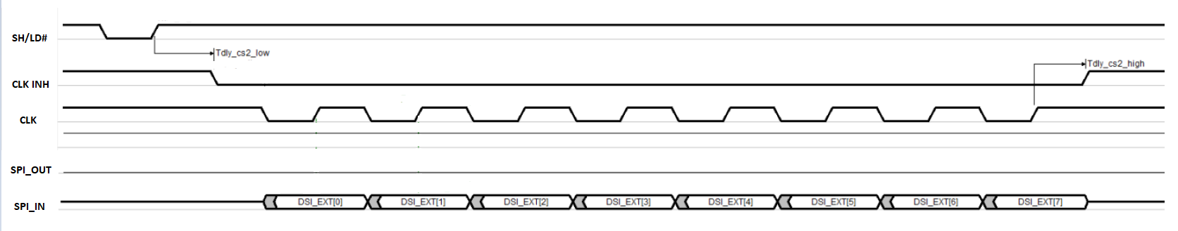
Can you please give more details regarding:

  • The minimum CLK INH output delay from SH/LD# rising edge (Tdly_cs2_low)
  • The minimum desabling delay of the CLK INH output following the last falling edge of the clock (Tdly_cs2_high)

Thanks and best regards

  • Hi,

    I'm not sure I fully understand what you're asking here.

    The minimum CLK INH output delay from SH/LD# rising edge (Tdly_cs2_low)

    CLK INH and SH/¯L¯D¯ are both inputs. There is no minimum time between SH/¯L¯D¯ going high and CLK INH going low specified in the datasheet, so this can happen simultaneously.

    • The minimum desabling delay of the CLK INH output following the last falling edge of the clock (Tdly_cs2_high)

    Since the CLK and CLK INH pins are interchangeable, the way you have the CLK INH rising after the CLK is held high will be fine. You may assume that the setup time parameter in section 6.7 of the datasheet labelled CLK INH before CLK↑ can also apply to this case.

    Thanks!

    Chad Crosby

  • Thanks Chad, this answer is helpful for my customer!