This thread has been locked.

If you have a related question, please click the "Ask a related question" button in the top right corner. The newly created question will be automatically linked to this question.

AM2432: OSPI sequence read operation to increase throughput

Part Number: AM2432

Tool/software:

Hello,

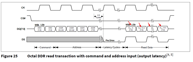
Take this OSPI flash as example. in the read timing figure, there are several sequenced data cycle after command, address, dummy cycle. In this way can read in multiple data in burst automatically. 

https://www.infineon.com/dgdl/Infineon-S28HS512T_S28HS01GT_S28HL512T_S28HL01GT_512MB_1GB_SEMPER_TM_FLASH_OCTAL_INTERFACE_1_8V_3-DataSheet-v68_00-EN.pdf?fileId=8ac78c8c7d0d8da4017d0ee6bca96f97

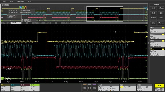
Also captured similar waveform on board.

But seems the burst read is not be used by software. 

When read 10 byte data in software, OSPI output 10 CS, each CS period has command, address, dummy cycle, and 5 DQS cycle. 

If read 8 byte data, then output 8 CS period. 

deep look into code, software use memcpy to read, OSPI should be in memory map mode already.

From the waveform, as there are 5 DQS signal, flash output 10 byte data within one CS period already, but software don't know, still read byte by byte.

With this timing behavior, the throughput is very poor, waste too many cycles, even lower than single line SPI as it has not dummy cycle required. 

#1. How to utilize the sequence read to increase throughput? Can only use DMA to utilize the sequency burst read?

#2. Is the 5 DQS configurable? we saw it is always 5 sequence pulse no matter how many byte to read.

  • Hi,

    #1. How to utilize the sequence read to increase throughput? Can only use DMA to utilize the sequency burst read?

    The waveforms observed by the customer, is seen at our setup as well. So this is something we are seeing at our TI EVM setup as well.

    Moreover, the DMA is utilized when the number of bytes to be read is greater than equal to 1024 bytes. Let me check the behaviour when DMA is enabled for transfer of lets suppose 1 kb of data. I will check the waveform for this and let you know if I see any improvement.

    #2. Is the 5 DQS configurable? we saw it is always 5 sequence pulse no matter how many byte to read.

    I did not have the DQS line configured to be probed, so could not see this behaviour.

    Please let me know if the customer is looking forward to INDAC reads? INDAC reads we saw that the entire operation lets say transfer of 256 bytes happens under 1 chip select.

    Regards,

    Vaibhav

  • Hi,

    When read 10 byte data in software, OSPI output 10 CS

    This is not seen in case of DMA reads, so for example, I lowered the limit of DMA copy and tested reading 256 bytes of data, and the number of CS is quite less as seen on the waveform for me. It is not 256 CS but around 8-9 CS.

    The way to change the lower limit of DMA copy is simply going to the file named ospi_v0.c and changing the value of the macro:

    #define OSPI_DMA_COPY_LOWER_LIMIT     (128U) // 1024
    I changed it to 128 bytes meaning that the transfer size has to be > 128 bytes to initiate DMA transfer.
    Just rebuild the libraries and then see the waveform for the same.
    Regards,
    Vaibhav
  • Hi Vaibhav,

    This is not seen in case of DMA reads

    I agree DMA will pipeline the burst. 

    Can CPU accessing take advantage of the burst feature of the interface?

    I changed it to 128 bytes meaning that the transfer size has to be > 128 bytes to initiate DMA transfer.

    Is there reason select 1024 to separate DMA and CPU accessing? DMA doesn't behave better than CPU if size<1024? or just leave one configurable size option?

    INDAC reads we saw that the entire operation lets say transfer of 256 bytes happens under 1 chip select.

    Is there a waveform to help understanding?

  • Hi,

    DMA doesn't behave better than CPU if size<1024?

    That is correct understanding but you can experiment with the configurable size as well.

    Is there a waveform to help understanding?

    I can share the waveform I have for 128 bytes of data. 

    Here you go: 

    Waveforms for different protocols: https://e2e.ti.com/support/processors-group/processors/f/processors-forum/1450567/am6421-ospi-frame-is-split/5683140#5683140

    Waveform for protocol 8D-8D-8D: https://e2e.ti.com/support/processors-group/processors/f/processors-forum/1450567/am6421-ospi-frame-is-split/5683367#5683367

    Regards,

    Vaibhav

  • Customer verified =<256byte will be only one CS with INDAC, >256 will split to multiple CS due to FIFO from code, but did not find much detail information about FIFO size of OSPI interface.

  • Hi Tony,

    I understand that the customer saw this behaviour.

    Can you suggest the customer to go ahead and modify the OSPI_readIndirect API as follows.

    If customer is on latest SDK:

    int32_t OSPI_lld_readIndirect(OSPILLD_Handle hOspi, OSPI_Transaction *trans)
    {
        int32_t status = OSPI_SYSTEM_SUCCESS;
        const CSL_ospi_flash_cfgRegs *pReg;
        uint8_t *pDst;
        uint32_t addrOffset;
        uint32_t remainingSize;
        uint32_t readFlag = 0U;
        uint32_t sramLevel = 0, readBytes = 0;
        OSPILLD_InitHandle hOspiInit;
    
        /* Check if hOspi & OSPI_transactions are NULL */
        if((NULL != hOspi) && (NULL != trans))
        {
            pReg = (const CSL_ospi_flash_cfgRegs *)(hOspi->baseAddr);
            hOspiInit = hOspi->hOspiInit;
            addrOffset = trans->addrOffset;
            pDst = (uint8_t *) trans->buf;
    
            OSPI_disableInterrupt(hOspi);
            OSPI_clearInterrupt(hOspi);
            if(TRUE == hOspi->hOspiInit->intrEnable)
            {
                OSPI_enableInterrupt(hOspi);
                hOspi->currTrans->addrOffset = trans->addrOffset;
                hOspi->currTrans->buf = trans->buf;
                hOspi->currTrans->count = trans->count;
                hOspi->currTrans->dataLen = trans->dataLen;
                hOspi->currTrans->transferOffset = 0U;
                hOspi->currTrans->state = OSPI_TRANS_READ;
                hOspi->currTrans->status = trans->status;
            }
    
            /* Disable DAC Mode */
            CSL_REG32_FINS(&pReg->CONFIG_REG,
                        OSPI_FLASH_CFG_CONFIG_REG_ENB_DIR_ACC_CTLR_FLD,
                        0U);
            CSL_REG32_WR(&pReg->IND_AHB_ADDR_TRIGGER_REG, 0);
    
            /* Config the Indirect Read Transfer Start Address Register */
            CSL_REG32_WR(&pReg->INDIRECT_READ_XFER_START_REG, addrOffset);
    
            /* Set the Indirect Write Transfer Start Address Register */
            CSL_REG32_WR(&pReg->INDIRECT_READ_XFER_NUM_BYTES_REG, trans->count);
    
            /* Set the Indirect Write Transfer Watermark Register */
            CSL_REG32_WR(&pReg->INDIRECT_READ_XFER_WATERMARK_REG,
                        CSL_OSPI_SRAM_WARERMARK_RD_LVL);
    
            // CHANGE INTRODUCED
            /* Set the SRAM Pariticion config reg read partition to fully 255, and write partition becomes 0. Earlier this value was set to 63. */
            CSL_REG32_WR(&pReg->SRAM_PARTITION_CFG_REG,
                        255);
    
            /* Start the indirect read transfer */
            CSL_REG32_FINS(&pReg->INDIRECT_READ_XFER_CTRL_REG,
                        OSPI_FLASH_CFG_INDIRECT_READ_XFER_CTRL_REG_START_FLD,
                        1);
    
            if(OSPI_TRANSFER_MODE_POLLING == hOspi->transferMode)
            {
                remainingSize = trans->count;
    
                while(remainingSize > 0U)
                {
                    if(OSPI_waitReadSRAMLevel(pReg, &sramLevel) != 0)
                    {
                        /* SRAM FIFO has no data, failure */
                        readFlag = 1U;
                        status = OSPI_SYSTEM_FAILURE;
                        trans->status = OSPI_TRANSFER_FAILED;
                        break;
                    }
    
                    readBytes = sramLevel * CSL_OSPI_FIFO_WIDTH;
                    readBytes = (readBytes > remainingSize) ? remainingSize : readBytes;
    
                    /* Read data from FIFO */
                    OSPI_readFifoData(hOspiInit->dataBaseAddr, pDst, readBytes);
    
                    pDst += readBytes;
                    remainingSize -= readBytes;
                }
                /* Wait for completion of INDAC Read */
                if(readFlag == 0U && OSPI_waitIndReadComplete(pReg) != 0)
                {
                    readFlag = 1U;
                    status = OSPI_SYSTEM_FAILURE;
                    trans->status = OSPI_TRANSFER_FAILED;
                }
    
            }
        }
        else
        {
            status = OSPI_LLD_INVALID_PARAM;
        }
        // Reverting back to default value.
        CSL_REG32_WR(&pReg->SRAM_PARTITION_CFG_REG,
                    63);
    
        return status;
    }

    If the customer is on a bit older SDK:

    int32_t OSPI_readIndirect(OSPI_Handle handle, OSPI_Transaction *trans)
    {
        int32_t status = SystemP_SUCCESS;
        const OSPI_Attrs *attrs = ((OSPI_Config *)handle)->attrs;
        OSPI_Object *obj = ((OSPI_Config *)handle)->object;
        const CSL_ospi_flash_cfgRegs *pReg = (const CSL_ospi_flash_cfgRegs *)(attrs->baseAddr);
        uint8_t *pDst;
        uint32_t addrOffset;
        uint32_t remainingSize;
        uint32_t readFlag = 0U;
        uint32_t sramLevel = 0, readBytes = 0;
        uint32_t dacState;
    
        addrOffset = trans->addrOffset;
        pDst = (uint8_t *) trans->buf;
    
        /* Disable DAC Mode */
        dacState = obj->isDacEnable;
        if(dacState == TRUE)
        {
            OSPI_disableDacMode(handle);
        }
    
        /* Config the Indirect Read Transfer Start Address Register */
        CSL_REG32_WR(&pReg->INDIRECT_READ_XFER_START_REG, addrOffset);
    
        /* Set the Indirect Write Transfer Start Address Register */
        CSL_REG32_WR(&pReg->INDIRECT_READ_XFER_NUM_BYTES_REG, trans->count);
    
        /* Set the Indirect Write Transfer Watermark Register */
        CSL_REG32_WR(&pReg->INDIRECT_READ_XFER_WATERMARK_REG,
                     CSL_OSPI_SRAM_WARERMARK_RD_LVL);
    
        // CHANGE INTRODUCED
        /* Set the SRAM Pariticion config reg read partition to fully 255, and write partition becomes 0. Earlier this value was set to 63. */
        CSL_REG32_WR(&pReg->SRAM_PARTITION_CFG_REG,
                    255);
    
        /* Start the indirect read transfer */
        CSL_REG32_FINS(&pReg->INDIRECT_READ_XFER_CTRL_REG,
                       OSPI_FLASH_CFG_INDIRECT_READ_XFER_CTRL_REG_START_FLD,
                       1);
    
        if(OSPI_TRANSFER_MODE_POLLING == obj->transferMode)
        {
            remainingSize = trans->count;
    
            while(remainingSize > 0U)
            {
                if(OSPI_waitReadSRAMLevel(pReg, &sramLevel) != 0)
                {
                    /* SRAM FIFO has no data, failure */
                    readFlag = 1U;
                    status = SystemP_FAILURE;
                    trans->status = OSPI_TRANSFER_FAILED;
                    break;
                }
    
                readBytes = sramLevel * CSL_OSPI_FIFO_WIDTH;
                readBytes = (readBytes > remainingSize) ? remainingSize : readBytes;
    
                /* Read data from FIFO */
                OSPI_readFifoData(attrs->dataBaseAddr, pDst, readBytes);
    
                pDst += readBytes;
                remainingSize -= readBytes;
            }
            /* Wait for completion of INDAC Read */
            if(readFlag == 0U && OSPI_waitIndReadComplete(pReg) != 0)
            {
                readFlag = 1U;
                status = SystemP_FAILURE;
                trans->status = OSPI_TRANSFER_FAILED;
            }
    
        }
    
        // Reverting back to default value.
        CSL_REG32_WR(&pReg->SRAM_PARTITION_CFG_REG,
                    63);
    
        /* Return to DAC mode if it was initially in enabled state */
        if(dacState == TRUE)
        {
            OSPI_enableDacMode(handle);
        }
    
        return status;
    }

    What this will make sure is that the transaction(which I have tested upto 512 bytes) happens under 1 chip select.

    In short, I am modifying the SRAM partition configuration register, where we allocate more space to read partition and then reset back to the default value of 63.

    Please read the comments in the code which is applicable for the customer's current development environment.

    Regards,

    Vaibhav

  • Hi Vaibhav,

    When will it update to AM64x, AM62x, AM24x MCU SDK?

  • Greetings Tony,

    Good to be back on this thread.

    Hi Vaibhav,

    When will it update to AM64x, AM62x, AM24x MCU SDK?

    Did my logic worked for the customer under 1 chip select? Like the transaction happened under 1 chip select? If Yes, then I would like to inform that this is more of a modification which depends on various requirements of a specific customer.

    INSIDE CODE CHANGES:

    This is essentially a way to say how much space has to be reserved for OSPI Indirect Write VS Read operations. This is configurable based on the requirement.

    For example, if I am not supposed to write a lot and read pretty less number of bytes, then I would allocate more to write and less to read to fasten up on things, or atleast make sure that the transactions happens under 1 chip select.

    Let me know your views on this.

    Conclusion:

    This cannot go into the SDK as it is just a small hack which can be carried from the customer's end as well after testing out a for a bunch of cycles.

    Regards,

    Vaibhav