


Part Number: MSP432P401R
Hello, my project idea is to rotate a BLDC motor by imposing a certain duty cycle value (which I change with Launchpad buttons) and setting a period value (in this case 1 ms) that allows me to make transitions between 6 states where in each state a high transistor and a low transistor are turned on at the same time while the other 4 transistors are turned off. The transitions are as follows:
State 1: high transistor of phase A and low transistor of phase B are on.
State 2: high transistor of phase A and low transistor of phase C are on.
State 3: high transistor of phase B and low transistor of phase C are on
State 4: high transistor of phase B and low transistor of phase A are on
State 5: high transistor of phase C and low transistor of phase A are on
State 6: high transistor of phase C and low transistor of phase B are on
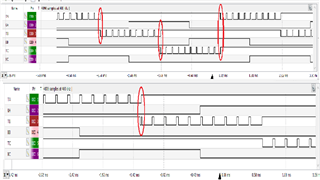
For the high transistors I have applied a PWM type signal and for the low transistors a GPIO signal that is simply held high or low, all depending on the state. My problem is that, although the transitions are done correctly (as I have been able to observe in the Analog Discovery that I use to visualize the time signal), I get a certain Jitter that makes me overlap transistor switching that should not be seen, marked with red circles in the image (as they belong to different states) and that, therefore, would cause that if I connect the motor there may be moments of time when I have 4 transistors working and will cause me big problems. To sum up, I would really like that there would not be any possibility of transistors overlapping between states and maybe even that there would be a certain short delay to make sure of it at each transition, but I can't think how to do it. I copy my code in case someone is able to tell me where the failure could be or what solution could solve it. Thanks in advance.
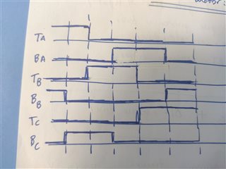
How transitions should be:
What I am getting on the Analog Discovery:
My code is the following:
-
#include "msp.h"
-
#include <stdint.h>
-
#include <stdio.h>
-
-
#define PWM 0x70 // 0111 0000
-
#define GPIO 0x07 // 0000 0111
-
volatile uint8_t estado = 0;
-
volatile uint8_t duty_cycle_inv = 150; // By setting this value we get approximately 50% Duty Cycle
-
-
void pulsadores(void){ // Use pushbuttons S2 (P1.4) and S1 (P1.1) to increase or decrease Duty Cycle by 10% respectively.
-
P1SEL0 &= ~(BIT4 | BIT1); // I/O
-
P1SEL1 &= ~(BIT4 | BIT1);
-
P1DIR &= ~(BIT4 | BIT1);
-
P1REN |= (BIT4 | BIT1);
-
P1OUT |= (BIT4 | BIT1);
-
P1IES |= (BIT4 | BIT1);
-
P1IFG &= ~(BIT4 | BIT1);
-
P1IE |= (BIT4 | BIT1);
-
}
-
-
void inicializaciones(void){
-
/* TA: P7.4; TB: P7.5; TC: P7.6
-
* BA: P7.0; BB: P7.1; BC: P7.2
-
*/
-
// Pines Transistores HIGH (PWM) // We configure pins P7.4 (TA1.4), P7.5 (TA1.3) and P7.6 (TA1.2) for Timer output.
-
P7SEL0 |= PWM;
-
P7SEL1 &= ~PWM;
-
P7DIR |= PWM;
-
-
// Pines Transistores LOW (GPIO)
-
P7SEL0 &= ~GPIO;
-
P7SEL1 &= ~GPIO;
-
P7DIR |= GPIO;
-
}
-
-
void TimerA1_PWM(void){ // Timer to control the 3 PWM pins
-
TA1CCR0 = 299; // (300-1) PWM Tperiod: 10 us -> As SMCLK = 3MHz, the counter counts in Up Mode every 1/3MHz = 0.333us. Therefore, 300 - 0.333us = 100 us
-
TA1CTL |= TASSEL_2 | MC_3 | TACLR; // SMCLK clock with a frequency of 3 MHz; MC_3: Up-Down Mode; TACLR: Clear TA1R register
-
TA1CCTL2 |= OUTMOD_6; // Modo CCR2: Toggle/Set
-
TA1CCTL3 |= OUTMOD_6; // Modo CCR3: Toggle/Set
-
TA1CCTL4 |= OUTMOD_6; // Modo CCR4: Toggle/Set
-
}
-
-
void TimerA0(void){
-
// This timer will be used to change states during the sequence.
-
TA0CCR0 = 374; // (375-1) PWM period: 1 ms
-
TA0CTL |= TASSEL_2 | ID_3 | MC_1 | TACLR; // SMCLK clock with a frequency of 3 MHz and with a frequency divider of 8, Up Mode
-
TA0CCTL0 |= CCIE; // Enables interrupts when the value of TA0CCR0 is reached.
-
}
-
-
void TimerA2_Antirebotes(void){
-
TA2CCR0 = 1023; // (1024-1) To obtain 250 ms of anti-rebounds -> The counter counts in Up Mode every 1/(4.096 kHz) = 0.244 ms. Therefore, 1024 - 0.244 ms = 250 ms
-
TA2CTL |= TASSEL_1 | ID_3 | MC_1 | TACLR; // ACLK clock with a frequency of 32.768 kHz and with a frequency divider of 8, Up Mode -> fACLK = 4.096 kHz
-
}
-
-
void init_interrupciones(void){
-
NVIC_EnableIRQ(TA0_0_IRQn);
-
NVIC_EnableIRQ(TA2_0_IRQn);
-
NVIC_EnableIRQ(PORT1_IRQn);
-
__enable_irq(); // Enable global interrupt
-
}
-
-
void main(void)
-
{
-
WDT_A->CTL = WDT_A_CTL_PW | WDT_A_CTL_HOLD; // stop watchdog timer
-
pulsadores();
-
inicializaciones();
-
TimerA1_PWM();
-
TimerA0();
-
TimerA2_Antirebotes();
-
init_interrupciones();
-
-
while(1){
-
switch(estado){
-
case 0: { // TA y BB HIGH
-
TA1CCR4 = duty_cycle_inv; // TA HIGH
-
TA1CCR3 = 0;
-
TA1CCR2 = 0;
-
P7OUT |= BIT1; // 0000 0010, as P7.1 (BB) será HIGH
-
break;
-
}
-
case 1: { // TA y BC HIGH
-
TA1CCR4 = duty_cycle_inv; // TA HIGH
-
TA1CCR3 = 0;
-
TA1CCR2 = 0;
-
P7OUT |= BIT2; // 0000 0100, as P7.2 (BC) será HIGH
-
P7OUT &= ~BIT1;
-
break;
-
}
-
case 2: { // TB y BC HIGH
-
TA1CCR4 = 0;
-
TA1CCR3 = duty_cycle_inv; // TB HIGH
-
TA1CCR2 = 0;
-
break;
-
}
-
case 3: { // BA y TB HIGH
-
TA1CCR4 = 0;
-
TA1CCR3 = duty_cycle_inv; // TB HIGH
-
TA1CCR2 = 0;
-
P7OUT |= BIT0; // 0000 0001, as P7.0 (BA) será HIGH
-
P7OUT &= ~BIT2;
-
break;
-
}
-
case 4: { // BA y TC HIGH
-
TA1CCR4 = 0;
-
TA1CCR3 = 0;
-
TA1CCR2 = duty_cycle_inv; // TC HIGH
-
break;
-
}
-
case 5: { // BB y TC HIGH
-
TA1CCR4 = 0;
-
TA1CCR3 = 0;
-
TA1CCR2 = duty_cycle_inv; // TC HIGH
-
P7OUT |= BIT1; // 0000 0010, as P7.1 (BB) será HIGH
-
P7OUT &= ~BIT0;
-
break;
-
}
-
}
-
}
-
}
-
-
void TA0_0_IRQHandler(void){ // Interrupt Timer A0
-
TA0CCTL0 &= ~CCIFG;
-
estado++; // we change state
-
if(estado > 5){
-
estado = 0;
-
}
-
}
-
-
void TA2_0_IRQHandler(void){ // Interrupt Timer A2
-
TA2CCTL0 &= ~CCIFG;
-
P1IFG &= ~(BIT4 | BIT1); // we lower the flag of the pushbutton so that it does not remain depressed
-
P1IE |= BIT4; // We reactivate interruptions on pushbutton P1.4
-
P1IE |= BIT1;
-
}
-
-
void PORT1_IRQHandler(void) // Interrupt Port P1
-
{
-
if(P1IFG & BIT4){ // With pushbutton P1.4 we REDUCE the Duty Cycle
-
P1IE &= ~BIT4;
-
if(duty_cycle_inv >= 250){
-
duty_cycle_inv = 250;
-
}
-
else{
-
duty_cycle_inv += 10;
-
}
-
P1IFG &= ~BIT4; // we lower the flag so that it does not stay pressed down
-
}
-
else if(P1IFG & BIT1){ // With pushbutton P1.1 we INCREASE the Duty Cycle
-
P1IE &= ~BIT1;
-
if(duty_cycle_inv <= 80){
-
duty_cycle_inv = 80; // To make sure that we NEVER get a value less than zero
-
}
-
else{
-
duty_cycle_inv -= 10;
-
}
-
P1IFG &= ~BIT1;
-
}
-
TA2CCTL0 |= CCIE; // enable interrupt on Timer A2_0
-
}
