This thread has been locked.

If you have a related question, please click the "Ask a related question" button in the top right corner. The newly created question will be automatically linked to this question.

TM4C123GH6PZ: GPIO pin failed driving opto-coupler

Part Number: TM4C123GH6PZ

A GPIO pin used within specified capabilities failed low / sinking current.

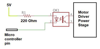
The pin is configured for PWM output with 8mA drive strength as required:

       GPIOPinConfigure(GPIO_PH2_WT5CCP0);
       GPIOPinTypeTimer(GPIO_PORTH_BASE, GPIO_PIN_2);
       MAP_GPIOPadConfigSet(GPIO_PORTH_BASE, GPIO_PIN_2, GPIO_STRENGTH_8MA, GPIO_PIN_TYPE_OD);

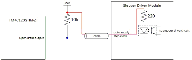
The pin is used as a low-side driver of an optocoupler on a separate PCB, circuit sketch below:

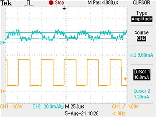
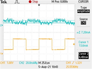
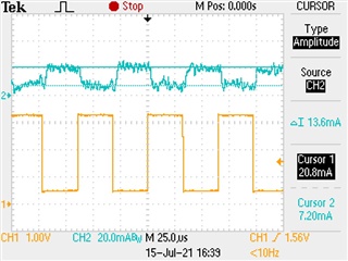
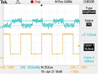
When the pin is driving the opto the following was measured on another (identical) copy of the board:

        Vout: 0.56V
        Iout: -16mA (into the pin)

The current measurement was confirmed under static conditions with a meter.

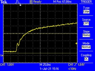
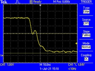
Scope screen captures:

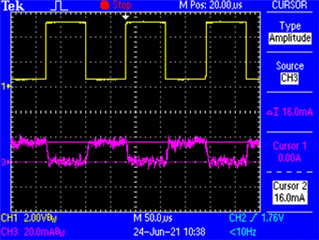
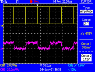
Driving the opto is intermittent, but when on the switching frequency is between 1Hz and 30kHz.  When idle the GPIO pin is pulled up to 5V.

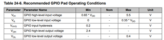
On one board the pin PH2 failed low, driving the opto.  The current sink capability specified in table 24-6 of the data sheet states up to 18mA at Vo = 1.2V.  We are well below that Vo level and below 18mA.

  • Hello John,

    Trying to understand a little more here. Is this occurring on just one board? And how many boards have been put under these conditions? Did the failure happen over time?

    Also when you said:

      Iout: -16mA (into the pin)

    I want to be sure I am understanding this right that the nomenclature used means that Iout was 16mA being output from the pin? I'm guessing here the -16ma is because the current tool was measuring in the opposite direction?

    Regardless, let me clear up an important point here...

    The current sink capability specified in table 24-6 of the data sheet states up to 18mA at Vo = 1.2V.  We are well below that Vo level and below 18mA.

    This is true, but the datasheet also includes another measurement. 8.0mA @ 8-mA drive for VOL = 0.4V which is much closer to your condition. Unfortunately, the datasheet does not provide maximum data, but I think it is important to understand there is a difference here between VOL = 0.4V and VOL = 1.2V specs.

    My first thought based on this is that maybe that is what is measured now but perhaps some sort of overvoltage or current impacted the pin.

    Another would be if there are multiple current sink/source on one side of the package which would go up against the restrictions per side of the package listed in Table 24-7.

    Also while the I/O are 5V tolerant, I'm a little concerned about the idea of an output line being pulled up to 5V because it should be trying to output 3.3V... I can't say I've seen anyone do that before.

    Best Regards,

    Ralph Jacobi

  • Hi Ralph,

    May thanks for the quick and thorough response, it's much appreciated.  Sorry to be imprecise and incomplete, let me clarify.

    The failure has been definitively identified on one board, others are suspected but not confirmed.  The known failure did happen after the board was in service for some time but I don't know precisely how long.  There are roughly a thousand similar units put into use over the last 5 years.

    When the pin is active (low), driving the opto-coupler it is sinking 16ma.  Seeing it now I can tell that what I intended to be emphasis actually looks like a double negative.  You are correct about the inversion of the current waveform on the scope captures.  I'd grown accustomed to the display and failed to notice it would be confusing.  Sorry about that.

    There was some debate here about the meaning of the 8mA@0.4V vs. the 18mA@1.2V spec.  The belief is that up to 18mA can be sunk by the pin as long as VOL is below 1.2V that voltage.  I get the sense that we may not be interpreting that correctly, please advise.

    Re the overvoltage/current impact on the pin, the measurements were made on a correctly functioning copy of the board, not the defective one.  Is that what you meant?

    We use 4 pins total in the same drive configuration.  2 pins are PWM'd as described to control the stepper motor speed, and the other two are essentially steady level to control direction of stepper motors (they are not driving the stepper directly, they drive control signals on a motor driver board per the opto schematic snippet provided above).  The PWM pins are #18 and 19 (100 pin package) and the direction control pins are 37 and 39.  All other loads are IC inputs or transistor gate pins, so very low current.  Is the fact that the 2 PWM pins are adjacent a concern?

    The PWM pins are configured as open-drain and pulled up to 5V through 10K resistors.  Is this configuration outside the pin's 5V tolerance?

    Thanks again, let me know if anything more is needed.

    John

  • Hi John,

    The PWM pins are configured as open-drain and pulled up to 5V through 10K resistors.  Is this configuration outside the pin's 5V tolerance?

    I'm checking this with a colleague but after delving into that element further, my gut is that it is okay because the datasheet indicates static voltages are tolerated at 5V even when MCU is off, and open drain shouldn't be impacted by that either.

    he PWM pins are #18 and 19 (100 pin package) and the direction control pins are 37 and 39.  All other loads are IC inputs or transistor gate pins, so very low current.  Is the fact that the 2 PWM pins are adjacent a concern?

    That should be fine from a current draw spec standpoint then, though the adjacent pins is something to keep in mind here for some of the below comments.

    Re the overvoltage/current impact on the pin, the measurements were made on a correctly functioning copy of the board, not the defective one.  Is that what you meant?

    Understood, thanks for clarifying this. I had been thinking that a prior event damaged the pin and caused the unusual measurements and that sinking 16mA was behavior after the failure occurred.

    There was some debate here about the meaning of the 8mA@0.4V vs. the 18mA@1.2V spec.  The belief is that up to 18mA can be sunk by the pin as long as VOL is below 1.2V that voltage.  I get the sense that we may not be interpreting that correctly, please advise.

    I will try! I am not a designer so it's a little difficult for me too, but here is how I was interpreting the specs in the datasheet:

    • At VOL of 0.4V in 8-mA Drive mode, the minimum current able to be sunk is 8mA
    • At VOL of 1.2V in 8-mA Drive mode, the minimum current able to be sunk is 18mA
    • To have 18-mA sink current loading, the VOL is supposed to be = 1.2V. 
    • The situation here is that you are at 0.56V for 16mA being sunk. This means you are much closer to where the minimum is only 8mA, not 18mA. As the specifications don't have a maximum the issue could be that too much current is being sunk for that voltage level.

    I think you have avoided any issues with the pin choices, but check through this note from the datasheet (which also shows the above segment):

    For special high-current applications, the GPIO output buffers may be used with the following restrictions. With the GPIO pins configured as 8-mA output drivers, a total of four GPIO outputs may be used to sink current loads up to 18 mA each. At 18-mA sink current loading, the VOL value is specified as 1.2 V. The high-current GPIO package pins must be selected such that there are only a maximum of two per side of the physical package with the total number of high-current GPIO outputs not exceeding four for the entire package.

    The failure has been definitively identified on one board, others are suspected but not confirmed.  The known failure did happen after the board was in service for some time but I don't know precisely how long.  There are roughly a thousand similar units put into use over the last 5 years.

    Thanks for the full background here, always helps to know quantities, in production etc. 

    I have one more possible idea here which is the GPIO#10 errata item: https://www.ti.com/lit/pdf/spmz849

    A fast transition on any GPIO pin can switch on a low resistance path between the GPIO pin or the adjacent GPIO pins and ground potentially causing a high current draw.

    This condition has been observed when the signal at the device pin has a slew rate such that the rise time or fall time (measured from 10% to 90% of VDD) is faster than 2ns. The condition is more likely to occur at high temperatures or in noisy environments.

    Obvious 2ns is a very short period of time, but because this is based on 10-90% of VDD which is at 3.3V, I am just pondering here if the 5V pull-up with the 30 kHz PWM could manage to land in that window. Also not sure how the adjacent pins could be influencing this. Thoughts?

    Best Regards,

    Ralph Jacobi

  • Hi Ralph,

    Thanks for another quick and thorough response!

    The more I think about it the more I think VOL = 1.2 volts must be the maximum VOL at which you can sink 18mA. My reasoning is based on the associated power dissipation.

    At VOL = 1.2V and sinking 18mA, the pin/chip is dissipating about 22mW. At my observed combination of VOL = 0.56V and 16mA the power dissipated is just under 9mW. Clearly less stressful on the chip.

    Power dissipation is likely most of what’s behind the cumulative maximum GPIO current limitations, so it makes sense that the limitations on any particular pin would be based on the power dissipated. This is also supported by the constraint that no more than 2 pins per side of the chip and no more than 4 pins total can be used to sink such current, which is certainly related to total power dissipation.

    Another consideration is that VOL is typically a max spec, as shown in table 24-6 of the datasheet.  I.e. it identifies the highest voltage the chip will produce to represent a low level (under stated conditions of course). If it’s lower than that, great, no one cares, which is why there’s no min specified.

    Thanks for pointing out the transition time issue. The mention of “… or the adjacent GPIO pins…” definitely raised an eyebrow. My initial measurements indicate that the rise time is not an issue, but the fall time is quite fast. My current setup is not up to a precise measurement in the neighborhood of 2ns, but I’ll try to get a better measurement. In our application it would likely make sense to use the slew rate control feature on these pins anyway. Looking at table 24-29 in the datasheet suggests that using that feature would eliminate the concern. Do I have that right?

    Thanks again,

    John

  • Hi John,

    Thanks for pointing out the transition time issue. The mention of “… or the adjacent GPIO pins…” definitely raised an eyebrow. My initial measurements indicate that the rise time is not an issue, but the fall time is quite fast. My current setup is not up to a precise measurement in the neighborhood of 2ns, but I’ll try to get a better measurement. In our application it would likely make sense to use the slew rate control feature on these pins anyway. Looking at table 24-29 in the datasheet suggests that using that feature would eliminate the concern. Do I have that right?

    I'll be honest, I hadn't seen the slew rate control feature before despite my years working with this device. There isn't a lot of information on it, but it is brought up explicitly in the open-drain configuration, so I think that will help yeah. Only thing is that I would bet that was tested for Open Drain @ 3.3V and not 5V. I think it would be enough anyways, but something to keep in mind and cross check.

    I'll run by the power dissipation theory with my team tomorrow, reading what you said makes sense to me but want to get a couple more eyes on that front to make sure we are interpreting that accurately.

    Let me know when you find out about the slew rate measurement because that seems to be the leading candidate right now based on what I've seen.

    Best Regards,

    Ralph

  • Hi Ralph,

    I did transition time measurements on the stepper drive signal, shown in the screen captures below.  As I suspected the rise time is leisurely, as expected for a pulled up signal (as opposed to driven high).  The fall time is definitely quicker, but nowhere near 2ns.  I tried it both with and without the slew control enabled, but there was no perceptible difference.  Reviewing datasheet table 24-29 suggests that for this signal the slew rate is limited by other factors, although I just noticed now that the measurement is between 20% and 80% of VDD.  I have the cursors at 10% and 90% in the screen shots below.  Even so we'd still be in the 15ns neighborhood.

    I'll be interested to hear your thoughts on the power question.

    Enjoy the holiday weekend!

    John

  • Hi John,

    I'll delve into this more tomorrow as we are observing the holiday today. Though to answer on the power question, yes our consensus is that the current vs VOL specs on the datasheet are related to power dissipation at the I/O pins and thus the current/voltage you are observing would not be out of spec if its just on two pins on a given side.

    Best Regards,

    Ralph Jacobi

  • Hi John,

    I would say you seem to be clear of the errata as well, at least for standard operation. Unexpected noise can still trigger it, but I think we can move forward with other avenues. 

    Since we will have to delve another level deeper here to try and uncover the root cause, I have further questions about the state of the device that is observing the failure:

    1) Is it a periodic failure, occurs every time the pin is pulled low but can be recovered, or is the I/O permanently grounded.

    2) If not permanently grounded, what is needed to recover from the failure? If periodic, how frequent?

    3) If permanently grounded, what is the behavior with the other boards and how many others are there?

    4) Has an ABBA swap been done to see if the problem follows the device onto a known good board and that a known good IC fails on the failing PCB?

    One last spec I wanted to note though I am very doubtful you'd run into such a situation:

    If the voltage applied to a GPIO pad is in the high voltage range (5V +/- 10%) while VDD is not present, such condition should be allowed for a maximum of 10,000 hours at 27°C or 5,000 hours at 85°C, over the lifetime of the device.

    Why I am doubtful is that over a 5 year span, that basically means the device would have to have VDD not present but the 5V signal present for about 25% of its lifespan. But in the interest of no stone unturned...

    Best Regards,

    Ralph Jacobi

  • Hi Ralph,

    I appreciate the "no stone unturned" approach, but you are correct that we are nowhere near that 10,000 hour limit for 5V present without VDD present.  All the power supplies derive from the same input power, so while there is likely some difference in the times when each supply reaches its nominal level, this would be in the neighborhood of milliseconds per power cycle, so I'm comfortable ruling that out.

    In answer to your questions:

    1. It is a permanent, unrecoverable failure but it can't be described as "permanently grounded".  The square drive waveform is apparent, but the high state is only about 0.2 - 0.3V higher than the low state.  I apologize for not providing this detail sooner, which might have been helpful.  I'm relatively new to this issue myself and haven't personally observed it, so I'm collecting info from different sources.
    2. n/a
    3. There is one confirmed instance of this failure and "a handful" of suspected but not confirmed instances.  Again, sorry to be vague, but I'm sharing what information I have.
    4. We replaced the micro on the board with the failure with a new micro and correct operation was restored.  We did not take the step of installing the suspect micro on a known-good board.

    Please let me know if this sheds any light or raises any more questions.

    Thanks again,

    John

  • Hi John,

    Do you have a current measurement on I/O for the fail case both when idle and when driving a waveform?

    Also, can you do the following experiment to test if the I/O is shorted? This should be simple which is since the pin in open drain, put a pulldown resistor onto the pin as well to create a voltage divider. Then when it is High-Z we should see a voltage on the node unless the I/O is shorted.

    Since you already have a 220 ohm pull-up resistor to 5V, adding a second 220 ohm to ground would allow you to see if you measure 2.5V or 0V. Though usually we'd use a larger resistor value which you could do too... like for example, usually we would choose 1kohm or higher. But even if you use like a 4.7kohm on the bottom one then you should measure 5 * 4700 / (220 + 4700 ) which is close to 5V. If you measures close to 0V then it is a short instead.

    Best Regards,

    Ralph Jacobi

  • Hi Ralph,

    Sorry for the extended silence.  I was distracted by more urgent matters, and then by vacation ;)

    I'll try the tests and let you know the results.

    Thanks,

    John

  • Hi Ralph,

    The good news is I was finally able to get my hands on 2 boards that exhibit the failure mode and I've made some measurements on them.

    The bad news is it seems that the information I conveyed in my last post a few weeks ago was not correct.  Clearly the VOH values I stated then got mangled somewhere between the source and my post, but the "0.2 to 0.3V" I reported then is not supported by observation.  The VOH values on the 2 boards I tested is actually between 2V and 3.3V, so I can imagine that maybe the "point" was dropped in the verbal relay.  I apologize for the error.

    So it seems that the failure is not a short or near-short from the pin to ground, but a failure of the open-drain output to turn off completely.  I believe it continues to conduct enough current to keep the opto-isolator it drives active, effectively disabling the stepper motor since there are no transitions.

    I believe this obviates the pull-down test you described.  Let me know if you don't agree.

    The voltage and current measurements are summarized in the table below.  Scope screen shots follow.

    Board Pin VOH [V] VIL [V] IOH [mA] IOL [mA] Notes
    1002 Pan 2.6 0.5 7.20 16.80 Voltages read from scope screen capture
    1002 Tilt 2.08 0.56 6.40 13.60 Voltages read from scope cursors
    3004 Pan 3.3 0.5 7.20 20.80 Voltages read from scope screen capture
    3004 Tilt 3.1 0.5 4.00 16.00 Voltages read from scope screen capture

    Table notes:

    • All currents are into the pin.
    • "Pan" and "Tilt" refer to the 2 pins on the micro that exhibit the issue.  They are configured identically but drive independent stepper motor driver modules.
    • To stay ahead of the issue I've recalled boards with serial numbers ending in 5006 and 7008 ;)

    Scope captures for each pin:

    Fig 1 - Board 1002, Pan:

    Fig 2 - Board 1002, Tilt:

    Fig 3 - Board 3004, Pan:

    Fig 4 - Board 3004, Tilt:

    Again, I'm sorry about the errors in my earlier report.  Having examples in hand now should eliminate that possibility in the future.

    Thanks,

    John

  • Hello John,

    Not a huge issue, I think it still sent us down some good paths on what to look into and rule out etc.

    So reading the tables I have some areas I'd like to get clarity on.

    Board Pin VOH [V] VIL [V] IOH [mA] IOL [mA] Notes
    1002 Pan 2.6 0.5 7.20 16.80 Voltages read from scope screen capture
    1002 Tilt 2.08 0.56 6.40 13.60 Voltages read from scope cursors
    3004 Pan 3.3 0.5 7.20 20.80 Voltages read from scope screen capture
    3004 Tilt 3.1 0.5 4.00 16.00 Voltages read from scope screen capture

    For each measurement, the numbers reflect the high and low range of the square wave, correct? And from your point of view, the open drain can't pull it lower than 0.5V and therefore the stepper is not seeing a 'low transition' which is causing the issue?

    I want to understand this comment a bit better:

    a failure of the open-drain output to turn off completely.  I believe it continues to conduct enough current to keep the opto-isolator it drives active, effectively disabling the stepper motor since there are no transitions.

    The main reason I am trying to hone in on this assumption is because right now looking at the measurements, the only one that is out of spec is the Tilt signal on Board 1002 as VOH should be minimum 2.4V. 

    VIL assuming a 3.3V supply can range from 0 to 1.155V per datasheet:

    Best Regards,

    Ralph Jacobi

  • VIL assuming a 3.3V supply can range from 0 to 1.155V per datasheet:

    Since it looks like the problem is on an output pin, shouldn't the VOL (GPIO low-level output voltage) rather than VIL (GPIO low-level input voltage) datasheet value be used in the analysis?

    I think the confusion occurred because in the table of measurements results from John the "VIL [V]" column should actually be titled "VOL [V]".

  • Hi Chester,

    I see your point regarding the output configuration. Though the story does not change as much there. The datasheet table shows that VOL should be at 0.4V max which indicates that 0.5V is out spec.

    However, there is a note above the table regarding current sinking:

    With the GPIO pins configured as 8-mA output drivers, a total of four GPIO outputs may be used to sink current loads up to 18 mA each. At 18-mA sink current loading, the VOL value is specified as 1.2 V.

    That said, it does show then at the Board 3004 Pan signal is sinking more current than the device is spec'd for. That could be an issue here as overcurrent always opens up the potential for device damage.

    Best Regards,

    Ralph

  • Hi Ralph and Chester,

    Sorry for the confusion, I'll try to clarify.

    Yes, the label in the table I posted is incorrect.  It should have been "VOL".  The data in the table reflects the high and low voltages at the micro output pin while the stepper motor drive is active (i.e. while the micro is trying to make the motor move).

    Re the statement "failure of the open-drain output to turn off completely",  I should have emphasized that in this case low is on and high is off.  So I meant it looks like a failure to reach a high enough voltage so that no current would flow through the opto-isolator input stage of the stepper motor driver module the pin drives.

    To restate it, I believe that the micro pin voltage, always less than 3.3V, is low enough that there is always sufficient current through the opto LED to activate that circuit, resulting in the apparent absence of transitions from the motor driver module's perspective. 

    • Recall that the micro pin is pulled up to 5V.
    • I realize this is a stretch at 3.3V, for which the opto circuit diagram from the initial post, assuming Vf for the LED of 1.5V, gives only 0.91mA.  I haven't been able to find explicit specs of the minimum current needed to activate the input stage on the stepper motor driver module we're using.  I will share that info when I get it.

    Thanks all,

    John

  • Hello John,

    Okay thanks for the clarification here. I think there are two elements to this potentially...

    One is that we have a situation of the out of spec pin which is the Tilt signal on Board 1002 that is at 2.08 V when VOH should be minimum 2.4V. I will be reviewing this aspect with my team shortly.

    The second is that the device is only spec'd to give a minimum of 2.4V on VOH, and that is being followed in the other three cases. Which means that the device is in spec for those three situations and there is nothing I can really suggest that TM4C is inherently doing incorrectly here. That is obviously very troublesome for this system and could mean that the solution in this case would have to be redesigning the system slightly to account for that the voltage output could be as low as 2.4V. But I will also cross check this with my team for any ideas.

    Lastly, I will also go over any concerns about the measure on Board 3004 Pan signal which is sinking excess current from spec. If that occurred on the other signals too, it could be a situation where the device has suffered some damage due to out of spec current sink.

    Best Regards,

    Ralph Jacobi

  • One is that we have a situation of the out of spec pin which is the Tilt signal on Board 1002 that is at 2.08 V when VOH should be minimum 2.4V.

    John reported the output is set to open-drain with:

           GPIOPinConfigure(GPIO_PH2_WT5CCP0);
           GPIOPinTypeTimer(GPIO_PORTH_BASE, GPIO_PIN_2);
           MAP_GPIOPadConfigSet(GPIO_PORTH_BASE, GPIO_PIN_2, GPIO_STRENGTH_8MA, GPIO_PIN_TYPE_OD);

    With open-drain configured is the VOH specification relevant?

    This is on the assumption that the GPIO_PIN_TYPE_OD option takes effect if the pin is used for PWM rather than GPIO.

  • Hi Chester,

    A good question and one that came up in our discussion: The answer is no, the VOH isn't relevant here as it should just go up to the pull-up voltage. So something is incorrectly sinking current. More to come shortly but wanted to acknowledge that quickly.

    Best Regards,

    Ralph Jacobi

  • Hello John,

    In addition to my comments in reply to Chester about the datasheet spec for VOH not being applicable here as that is for when the TM4C MCU is driving the voltage output, a couple other ideas came back as we looked through this thread.

    1. The IOH current seems large for if the device is supposed to be in open drain mode and releasing the ground connection.
      1. The first thought that comes to mind is that the 10k resistor is too large and that a smaller resistor would draw less current and increase the voltage level
      2. However, this also is a challenge because a smaller resistor would then likely cause more current to be sunk by the device when the open drain pulls to ground, and some of these measures are dangerously close to the 18mA limit.
      3. Can you try and use Board 1002, Tilt pin to test decreasing the resistance and seeing what readings you get? Probably small decreases first so it doesn't suddenly spike in current and blow the I/O or something.
    2. On a similar line of thinking, can you measure what the input impendence is at the octo-isolator? The behavior seen looks like of like a voltage divider in some ways.
      1. Along similar lines, if you can try and measure the impendence of the TM4C pin when it is floating in open drain mode, that could also be useful here.
    3. The excessive current measurement is a bit concerning, is there any way to track the current draw over time as the PWM is running to see if there is any evidence of current overshoots?

    Basically the general takeaway is that something on the board is causing current to be sunk when the open drain pin releases the ground, and so this is trying to figure out what it is. And if its the micro that is causing that, then was it subjected to out of spec current levels that could have caused some damage to the device.

    Best Regards,

    Ralph Jacobi

  • Hi Ralph,

    A picture is worth 1024 words, so here's a sketch of the step drive circuit to save me getting too wordy:

    Re your comments:

    1. Using a smaller resistor in place of the 10k pull-up would certainly increase the voltage when the micro output is off (i.e. not conducting), but it would form a current divider with the opto circuit, diverting the current from where it's needed and increasing the total as you observed in (1.b).  And the issue is an anomaly, not a design question (almost all the boards work fine, with VOH very near 5V).  If I tried a test with a smaller pull-up, VOH would certainly be higher, but it's not clear to me how that would be informative.  Please advise if I'm missing something.
    2. I've requested more detailed info from the stepper driver module manufacturer, but no response yet.  Even so, I think we can ballpark that the impedance of the input circuit is 220 ohms in series with a small capacitance of the LED, which fits with the decay that's apparent in the rise and fall times reported above.
      1. This is the heart of the matter I think (per your summary too): it seems clear that the micro pin is sinking some current when we intend it not to.  Is there a failure mode in which the open drain output can fail to completely shut off?  If so, what conditions can cause such a failure mode?  The current overshoot mentioned in (3)?
    3. Would this test be conducted on a normal, working board or a failed one?  I'm afraid the current captures I provided in the scope screen shots above are near the limit of detail that can be obtained with our setup.  I had to average steady-state waveforms to get even those noisy captures.  If current overshoot is the likely cause of the issue I can look into how we might arrange to capture that level of detail.  Please let me know if that info is essential to settling this issue.

    Thanks again for your diligence in pursuing this, I appreciate it.

    John

  • Hi John,

    Is there a failure mode in which the open drain output can fail to completely shut off?  If so, what conditions can cause such a failure mode?  The current overshoot mentioned in (3)?

    There is no known fail mode in terms of errata or device specs for this, but current overshoot could certainly be an explanation. Once the max specs are violated, we no longer can guarantee that the device operation will follow the specs.

    In my experiences as an applications engineer, a lot of silicon is pretty durable. I've seen cases where small excursions of overcurrent or overvoltage does nothing to a large amount of devices but it's enough to cause fallout on a few, enough to make it an issue for production. This could be the case here where just a couple boards out of this run are having issues and the others are able to chug along. But with anything out of spec, the question that always linger is: For how long?

    Would this test be conducted on a normal, working board or a failed one?

    I think the failed one already shows pretty clearly it happened on it, so I would be curious for the normal board first I think. If even a functional board is generating overcurrent situations into the IO then that would be an indicator that the system is going to be stressing all micros. If the normal board does not exhibit that, then the next step probably would need to center on why the failed board does. Though I think there needs to be a sample size element to it too. I don't know how much tolerance of components etc. could play a role. But if its hard to do more than one at a time, start with a normal one and see where that gets us?

    If I tried a test with a smaller pull-up, VOH would certainly be higher, but it's not clear to me how that would be informative.  Please advise if I'm missing something.

    The thought here had more or less spawned from trying to come up with manners to increase the open-drain voltage so the stepper can resume proper operation. But if that draws excess current into the MCU when pulled low or doesn't provide enough current for the stepper, then that isn't viable. We aren't experts on motor drive applications so this was just an idea about how to possibly address the lower voltages being observed.

    Best Regards,

    Ralph Jacobi

  • Hi Ralph,

    After reviewing the status of this issue on our end and in light of the insights you've provided, we consider the matter to have been sufficiently investigated at this point, so I'll resolve the issue.

    An updated version of the circuit includes transistors between the micro and the stepper motor driver to free the micro pin from the job of sinking all the current required to drive the opto input of the stepper motor module.

    Thank you again for all your quick and helpful responses in addressing this.  I really appreciate it.

    Best of luck,

    John

  • Hi John,

    Thanks for the follow up and confirmation of the issue being resolved. Glad that we were able to get you the feedback needed so you could assess how our TM4C works in your system. This was definitely a tricky one and I learned a few things myself! Good luck with next version and let us know if there are any other issues.

    Best Regards,

    Ralph Jacobi