This thread has been locked.

If you have a related question, please click the "Ask a related question" button in the top right corner. The newly created question will be automatically linked to this question.

TM4C1294KCPDT: TM4C1294KCPDT

Part Number: TM4C1294KCPDT

お世話になります。

標記のTM4C1294KCPDTI3を使用した製品の設計中ですが、ハードリセットに付き確認したいです。
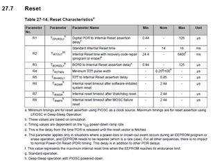
#69(RST)端子によるリセットではなく、パワーオンリセットは可能でしょうか?タイミング等、どこかに記載がありますでしょうか?

・#69(RST)端子を利用したハードリセットの仕様に付き、確認したいのですが、パルス幅の規定等、どこかに記載がありますでしょうか?

お忙しいところ恐縮ですが、ご回答のほどお願い致します。

以上です。

  • Hi,

      Please refer to the POR and nRST in the datasheet for detail. 

    5.2.2.3 Externally Generated Power-On Reset (POR)
    Note: The JTAG controller can be reset by a power-on reset or by holding the TMS pin to high
    for 5 clock cycles.
    During an externally generated POR, the internal Power-On Reset (POR) circuit monitors the power
    supply voltage (VDD) and generates a reset signal to all of the internal logic including JTAG when
    the power supply ramp reaches a threshold value (VPOR). Reset does not complete if specific voltage
    parameters are not met as defined in the Electrical Characteristics chapter. For applications that
    require the use of an external reset signal to hold the microcontroller in reset longer than the internal
    POR, the RST input may be used as discussed in “External RST Pin” on page 223. Holding this pin
    active can keep the initialization process from starting even though power-on reset has occurred.
    This is useful in in-circuit testing and other situations where it is desirable to delay the operation of
    the device until an external supervisor has released.
    The Power-On Reset sequence is as follows:
    1. The microcontroller waits for internal POR to go inactive.

    2. The internal reset is released and the core executes a full initialization of the device. Upon
    completion, the core loads from memory the initial stack pointer, the initial program counter,
    and the first instruction designated by the program counter, and then begins execution.
    The internal POR is only active on the initial power-up of the microcontroller, when the microcontroller
    wakes from hibernation, and when the VDD supply drops below the its defined operating limit. Please
    refer to the Electrical Characteristics chapter for information on exact values. The Power-On Reset
    timing is shown in “Power and Brown-Out” on page 1826.
    5.2.2.4 External RST Pin
    When the external RST pin is asserted it initiates a system reset or Power-On Reset depending on
    what has been configured in the Reset Behavior Control (RESBEHAVCTL) Register. If the EXTRES
    bit field in RESBEHAVCTL is set to 0x3 then a simulated full initialization will begin upon RST
    assertion. If these bits are programmed to 0x2 then a system reset is issued. When EXTRES is set
    to a 0x0 or 0x1, then the external RST pin performs its default operation upon assertion, which is
    issuing a full simulated POR.
    An external reset pin (RST) that is configured to generate a Power-On Reset resets the microcontroller
    including the core and all the on-chip peripherals. The external reset sequence is as follows:
    1. The external reset pin (RST) is asserted for the duration specified by TMIN and then deasserted
    (see “Reset” on page 1831). This generates an internal POR signal.
    2. The microcontroller waits for internal POR to go inactive.
    3. The internal reset is released and the core executes a full initialization of the device. Upon
    completion, the core loads from memory the initial stack pointer, the initial program counter,
    and the first instruction designated by the program counter, and then begins execution. Refer
    to “Reset” on page 1831 for internal reset deassertion timing.
    An external reset pin (RST) that is configured to generate a system reset will reset the microcontroller
    including the core and all the on-chip peripherals. The external reset sequence is as follows:
    1. The external reset pin (RST) is asserted for the duration specified by TMIN and then deasserted
    (see “Reset” on page 1831).
    2. The internal reset is released and the core loads from memory the initial stack pointer, the initial
    program counter, and the first instruction designated by the program counter, and then begins
    execution.
    Note: It is recommended that the trace for the RST signal must be kept as short as possible. Be
    sure to place any components connected to the RST signal as close to the microcontroller
    as possible.
    If the application only uses the internal POR circuit, the RST input must be connected to the power
    supply (VDD) through an optional pull-up resistor (0 to 100K Ω) as shown in Figure 5-1 on page 224.
    The RST input has filtering which requires a minimum pulse width in order for the reset pulse to be
    recognized, see Table 27-14 on page 1831.
    To improve noise immunity and/or to delay reset at power up, the RST input may be connected to
    an RC network as shown in Figure 5-2 on page 224. If the application requires the use of an external
    reset switch, Figure 5-3 on page 224 shows the proper circuitry to use. In the figures, the RPU and
    C1 components define the power-on delay. The external reset timing is shown in Figure
    27-11 on page 1832.