This thread has been locked.

If you have a related question, please click the "Ask a related question" button in the top right corner. The newly created question will be automatically linked to this question.

TMS570LS1224: How to read the MIBSPI5NCS[0] signal

Part Number: TMS570LS1224

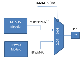
Hi, I don't understand how I can write code that will read the state of the MIBSPI5NCS[0] signal connected to pin 32 of the tms570.  I understand how this signal is similar to N2HET2[12], for example and I know that N2HET1[12], when configured as an output, can be toggled using:

gioToggleBit(hetPORT1, 12);

In deed, the previous level of support had ref'ed a similar question in which it was suggested that the following could be used:

gioSetBit(mibspiPORT5, bit_index, value)

However, although I guess I could replace "gioSetBit" with "gioGetBit" (something I've already considered) but confusion remains re MIBSPI5NCS[0]:

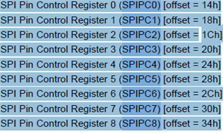
  1. The first thing that confuses me is that the address used in the def of mibspiPORT5 is the same as that for spiPORT5:
    #define mibspiPORT5 ((gioPORT_t *)0xFFF7FC18U
    #define spiPORT5 ((gioPORT_t *)0xFFF7FC18U)
  2. The 0xFFF7FC18 address points to SPIPC1 reg (offset 18h) and then the gioGetBit() fn's use of "port->DIN" gets us to SPIPC2 (offset 1Ch = 18h+4) but I don't understand what value to use for "port" in the call to gioGetBit().
  3. How do I ensure that MIBSPI5NCS[0] is configured as an input?
  4. Table 4-21 in the SPNU515C doc is the only place in this doc that ref's MIBSPI5NCS[0] but this table confuses the hell out me.
  • Hello Marcus,

    1. mibspiPORT5 is the same as spiPORT5

    2. You can use either of them. The SPIPC[5:1] (DIR, DIN,  DOUT, Dout_Set, Dout_Clear) are used only when the pin is configured as a GIO pin.

    3. If this pin (32) is configured as MibPSI5NCS[0] (PINMMR[3:0]=0x1), the MibPSI5NCS[0] can be used either SPI functional (CS[0]) or GIO. Writing 1 to SPICS0[0] is to use it as SPI functon pin (MIBSPINCS[0]), writing 1 to SPIPC0[1] is configured this pin as a GIO pin. 

        If MIBSPI5NCS[0] is used as a GIO pin, the SPIPC1[0] =0 means the pin is input. 

        If MIBSPI5NCS[0] is used as SPI CS[0] pin, the pin is input if MibSPI5 is configured as SPI slave. It is output if MibSPI5 is SPI master.

    4. In TMS570LS1224 144-pin package, the Pin 32 is used as MIBSPI5NCS[0] or EPWM4A. The Table 4-21 in TRM shows the pinmux configuration.

        Writing 0x1 to PINMMR27[3:0] is to configure pin 32 as MibPSI5NCS[0]

        Writing 0x2 to PINMMR27[3:0] is to configure pin 32 as EPWM4A

  • Thanks for the quick response to this query; unfortunately you may have underestimated the depths of my ignorance as your response opens up more questions - please forgive me if I'm a little pedantic but I'm trying to relate your answer to the TRM:

    =1========================================================================================================

    RE:

    3. If this pin (32) is configured as MibPSI5NCS[0] (PINMMR[3:0]=0x1), the MibPSI5NCS[0] can be used either SPI functional (CS[0]) or GIO. Writing 1 to SPICS0[0] is to use it as SPI functon pin (MIBSPINCS[0]), writing 1 to SPIPC0[1] is configured this pin as a GIO pin. 

    When you refer to "PINMMR[3:0]", did you really mean "PINMMR27[3:0]" as ref'ed in your bullet-point 4?

    =2========================================================================================================

    RE:

    Writing 0x1 to PINMMR27[3:0] is to configure pin 32 as MibPSI5NCS[0]

        Writing 0x2 to PINMMR27[3:0] is to configure pin 32 as EPWM4A

    What do you mean by "[3:0]"?  I would normally expect such indexing to be used to refer to specific bits within the specified register but I can't relate what you've written to Fig 4-17/Table 4-20 in the TRM.  In addition, there is the question of the damned Table 4-21: this must relate to this text as it too ref's PINMMR27 but in doing so it adds to my confusion by ref'ing PINMMR27[0], PINMMR27[1], PINMMR27[2], PINMMR27[3] and, more significantly PINMMR27[4].

    =3========================================================================================================

    RE:

    Writing 1 to SPICS0[0] is to use it as SPI functon

    I'm afraid I don't know what "SPICS0[0]" means in relation to the TRM; I was expecting something to do with the SPIPC0 reg (Table 28-13)

    =4========================================================================================================

    RE:

    writing 1 to SPIPC0[1] is configured this pin as a GIO pin

    This is looking better from perspective but the "[1]" bit confuses me: I could have got my head around something like "[7:0]" as Table 28-13 defines bits 7-0 as SCSFUN but even that I'm not sure about as I don't know what SCSFUN has to do specifically with MIBSOI5NCS[0].

    =5========================================================================================================

    RE:

    If MIBSPI5NCS[0] is used as a GIO pin, the SPIPC1[0] =0 means the pin is input. 

    The ref to "SPIPC1" gets me back to something I was close to understanding right back at the beginning but again, the indexing "SPIPC1[0]" confuses me; how does this relate to Table 28-14?  A selection of [7:0] might have made sense to me if only I knew the significance of "SCSDIR" with regard to MIBSOI5NCS[0].

  • Yes, it is PINMMR27. Each byte in the PINMMRs control the functionality output on a single terminal. From table 4-21 of TRM, PINMMR27[7:0] control the multiplexing between MIBSPI5NCS[0] and EPWM4A on the PIN 32. The default function on PIN 32 is MIBSPI5NCS[0] which is indicated by bit 0 of the PINMMR27 register being set.

    If you want to use PIN 32 as EPWM4A signal, bit 2 (bit 1 is not correct in my previous post) of PINMMR27 must be set and bit 0 must be cleared. Other bits of PINMMR27[7:0] are reserved.

    The MIBSPI5NC[0] can be used as SPI function pin or GIO pin, which can be configured via SPIPC0 register.

  • Thanks for the clarification re PINMMR27 and the selection of MIBSPI5NCS[0]; that just leaves us with the small matter of actually controlling this signal which I now believe to be the job of the SPIPCx regs and given that the objective is to monitor the state of the input signal, the SPIPCx set is reduced to the following sub-set:

    • SPIPC0: controls the function which I assume needs to be GIO (correct?)
    • SPIPC1: contols direction - simple enough, needs to be an input
    • SPIPC2: data in

    This would leave the issue resolved except the same question applies to all of the SPIPCx set: which bit correlates to the MIBSPI5NCS[0] signal?  Answering this question using the TRM appears to be next to impossible (well, fully impossible for me).  However, the following code in pinmux.h implies that the answer is bit 0:

    #define PINMUX_PIN_32_SHIFT                 0U

    #define PINMUX_PIN_32_MIBSPI5NCS_0           ((uint32)((uint32)0x1U <<  PINMUX_PIN_32_SHIFT))

    Please confirm.

  • The PINMMR27[7:0] is used to select signal for Pin 32: MIBSPI5NCS[0] or  EPWM4A. Bit 0 of PINMMR27 register is for MIBSPI5NCS[0], and Bit 2 is for EPWM4A.

    PINMMR27[7:0] = 0x01  --> Pin 32 is used for MIBSPI5NCS[0]  ---> MIBSPI5NCS[0]  (SPIPC0[0] = 1)

                                                                                                         ----> GIO (SPIPC0[0] = 0)

    PINMMR27[7:0] = 0x04  --> Pin 32 is used for EPWM4A

    SPIPC0: controls the function which I assume needs to be GIO (correct?)

    Yes, you are correct.

    which bit correlates to the MIBSPI5NCS[0] signal? 

    Bit 0 of SPIPC0 register is for nCS[0]

    Bit 1 of SPIPC0 is for nCS[1]

    Bit 2 of SPIPC0 is for nCS[2]

    ... ...

    Bit 8 of SPIPC0 is for SPI ENA pin

    Bit 9 of SPIPC0 is for SPI CLK pin

    ...

  • Hi QJ, thanks again for persisting with me.  I think we are really close to me closing this issue as "resolved" but, call be pedantic (in fact call me whatever you like), I'm stuck on your refs to "nCS[0], nCS[1] & nCS[2]" as such suffixes are applied to multiple signal in the TRM; can I simply assume:

    Bit 0 of every reg in the SPIPCx set:

    apply to MIBSPI5NCS[0]?  Simple as that!

    Marcus

  • Yes, your understanding is correct.

    Bit 0 of SPIPCx applies to MibSPIxNCS[0]

    Bit 1 of SPIPCx applies to MibSPIxNCS[1]

    ...

  • Hi, thanks for clarification.

    Marcus