This thread has been locked.

If you have a related question, please click the "Ask a related question" button in the top right corner. The newly created question will be automatically linked to this question.

TMS570LC4357: Internal RAM memory test in TMS570LC4357

Part Number: TMS570LC4357
Other Parts Discussed in Thread: HALCOGEN

Hi,

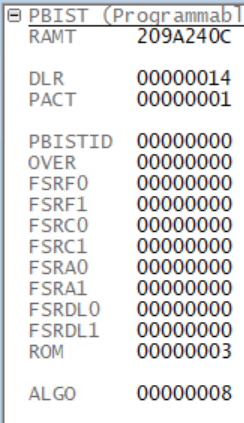
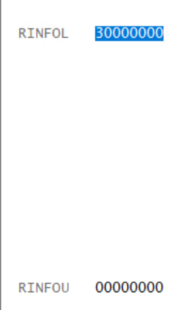
  • When the internal RAM memory test is performed using the March13N algorithm for Single-port considering the Groups 29 and 30 for L2RAMW, I am encountering L2RAMW - double-bit ECC uncorrectable error (Group 3 Channel 3 error) [sometimes, bus error also] which affects the further execution of application leading to an exception.

Referring to the C:\ti\Hercules\SafeTI Diagnostic Library\2.4.0\demo_app\common\source\app_main_NoOS.c, came accross the below statement:

"/* nERROR with PBIST_RAMGROUP_29_L2RAMW (PBIST_RAMGROUP_30_L2RAMW)
* Running PBIST on Cache memories need special considerations to be taken care
* of in application. */"

Please confirm if the PBIST memory test can be performed on the internal RAM test. (If it cannot be performed, please also clarify the reason)

What is the alternative to test the Internal RAM test and how can it be integrated into the PBIST sequence?

Also, what are the special considerations to be taken care of when PBIST is run on Cache memories? Please clarify.

  • This is regarding the PBIST tests: Referring to the demo code in C:\ti\Hercules\SafeTI Diagnostic Library\2.4.0\demo_app\HALCoGen\TMS570LC4357_NoOS\source, the sequence of built-in self-tests is not provided in the startup code. Request you to provide the exact sequence of built-in self-test to be followed.

Thanks

Tirumala.

  • Yes, the PBIST can be used to test the internal MCU RAM.

    The PBIST failure in the peripheral RAM or MCU SRAM will not generate ESM errors. When the PBIST is done, a PBIST done interrupt will be asserted.

    Please ensure that the MCU SRAM is initialized as the first operation after power-up before it is used.

  • Thanks, Wang. Will check it.

    Please clarify the special consideration of PBIST on Cache memories and also the sequence of all the BIT tests.

  • On LC4357, the memory group 31 and 32 are for I and D cache. 

    Please refer to "9.3.1 PBIST Sequence" of the TRM: SPNU563A

  • It is not about the sequence of steps for PBIST Self check.

    Please consider the query as:

    Considering all the BITS like PBIST self-check, PBIST STC ROM self-test, PBIST ROM self-test, STC self-test, CCM self-test, TPRAM self-test, L2RAMW ECC tests, Flash ECC tests, L2RAMW memory self-test, etc., what is the order of executing these tests. 

    Thanks,

    Tirumala.

  • I have initialized the SRAM before performing the memory test on it and it is leading to stack issues post initialization, although the stack initialization is done right before memory initialization.
    Could you please suggest the solution to the issue?

  • For Pbist self-check, please refer to the pbistSelfCheck() for TMS570LSx device, or refer to the similar function in safety diagnostic library (SDL).

    Considering all the BITS like PBIST self-check, PBIST STC ROM self-test, PBIST ROM self-test, STC self-test, CCM self-test, TPRAM self-test, L2RAMW ECC tests, Flash ECC tests, L2RAMW memory self-test, etc., what is the order of executing these tests. 

    Please read the TRM, and example code in SDL.

  • Thanks, Wang.

    Request you to provide the solution for this query.

    I have initialized the SRAM before performing the memory test on it and it is leading to stack issues post initialization, although the stack initialization is done right before memory initialization.
  • To be clear, after performing the memory initialization before and after the Internal SRAM test, the bus error is encountered.

  • Please find the screenshot attached, where this error is encountered while checking for the complete status of the PBIST internal RAM test.

  • There is one SW bug in pbiststop(). The pbistStop() function generated by HCG is missing a reset for the PBIST controller. The function below is the updated pbistStop(). Please update the routine generated by HALCoGen to match the following.

    void pbistStop(void)
    {
    /* USER CODE BEGIN (20) */
        pbistREG->PACT = 0x0U;
        systemREG1->MSTGCR &= 0xFFFFFFF0U;
        systemREG1->MSTGCR |= 0xAU;
        systemREG1->MSTGCR &= 0xFFFFFFF0U;
        systemREG1->MSTGCR |= 0x5U;
    /* USER CODE END */
    }
  • Yes, the same routine has been followed. The error is seen even before the stop_memory_test() is executed while checking for the completion of the test.

  • Does the memory group for PBIST test include any un-implemented memory group? for example USB memory. Can you post the value of the error flag? It would be helpful if you could share the code with me.

  • Hi Wang,

    Please find the attached snapshots of the configured registers to run a memory test on L2RAMW.

    After executing the PBIST, the error flags are seen as below:

    The code is running from the location 0x08000000h.

    The internal RAM memory test is performed after performing the STC self-check.

    The above error is seen while checking for the completion of the internal RAM memory self-test.

  • The code for the test is as below:

    volatile uint32* const sys_regs = reinterpret_cast<volatile uint32*>0xFFFFFF00);
    volatile uint32* const pbist_regs = reinterpret_cast<volatile uint32*>(0xFFFFE400);

    void main()

    {

    // Calls from main

    boolean test_status=false;

    execute_pbist(0x30000000, 0x00000004); // This performs the test and the configuration is as shown in snapshots attached in previous reply

    while(!(is_test_complete()); //Wait until test is complete 

    if((!is_test_passed()) || (!is_test_complete()))

    {

       test_status = true; 

    }

    return;

    }

    Bool is_test_complete()
    {
    return ((sys_regs[MSTCGSTAT] & 0x1UL) != 0UL);  //:MSTCGSTAT = 0x68
    }

    Bool is_test_passed()
    {
    return(0UL == (pbist_regs[FSRF0] & 0x1UL)); //FSRF0 = 0x190
    }

    In the highlighted code above, the code polls for the test complete. After having the call to is_test_complete() and returning back to main(), then the bus error is occurred. 

  • Kindly note that the above code is a replica of what we're implementing to perform the test and is run from location 0x08000000.

    Additionally, can you please let me know how to save the context before the test and retrieving the context after the test. Any code implementing the context saving would help us.

    Thank you,

    Tirumala.

  • When you perform PBIST on MCU SRAM, the content in stack area will be lost too. This is why the SRAM pbist test is performed in c_int00() generated by HALCoGen.

    I don't have an example code to save SRAM content. There are two SRAM groups: group 29 and group 30. You can run the pbist test for those 2 groups separately. When testing group 1, you can save its content to group 2 memory.

  • Can you please provide the memory ranges of both groups 29 and 30 for L2RAMW? Also, please provide the relation between RDS and RGS with the memory ranges of the L2RAMW.

    Thanks,

    Tirumala.

    • Hi Wang,

      There are two SRAM groups: group 29 and group 30. You can run the pbist test for those 2 groups separately. When testing group 1, you can save its content to group 2 memory.

      I have copied the content from 0x8000000 to 0x8040000 of size 0x3FFFF assuming that group 29 starts at 0x8000000v(L2RAMW) and group 30(L2RAMW ECC) at 0x8040000. Then ran the PBIST on Group 29 but still encountering the bus error. Please confirm if the ranges are correct along with the above query.

      Can you please provide the memory ranges of both groups 29 and 30 for L2RAMW? Also, please provide the relation between RDS and RGS with the memory ranges of the L2RAMW.

      -  As another try, I have tried executing PBIST on both the groups at the start of _c_int00() in SDL code as below:

      void _c_int00(void)
      {
      /* Initialize Core Registers to avoid CCM Error */
      SL_Init_R5Registers();

      /* Initialize Stack Pointers */
      SL_Init_StackPointers();

      /* Enable CPU Event Export */
      _SL_Init_EnableEventExport();

      /*Initialize RAM memory*/
      SL_Init_Memory(RAMTYPE_RAM);

      /*Perform BIST on RaAM group 29 and 30*/
      SL_SelfTest_PBIST( PBIST_EXECUTE, 0x30000000, PBISTALGO_MARCH13N_1PORT);

      /*Initialize RAM memory*/
      SL_Init_Memory(RAMTYPE_RAM);
      SL_PBIST_FailInfo failInfoPBISTOthers;
      while (TRUE != SL_SelfTest_Status_PBIST(&failInfoPBISTOthers));
      SL_SelfTest_PBIST_StopExec();
      SL_Init_R5Registers();
      SL_Init_StackPointers();
      _SL_Init_EnableEventExport();

      // The rest of the code is to execute based on the reset type given in SDL code

      }

      When this is tried, the code is stuck at the while loop 

      while (MEM_HW_INIT_COMPLETE != BF_GET(sl_systemREG1->MSTCGSTAT, BF_MINIDONE_START, BF_MINIDONE_LENGTH));

      in SL_Init_Memory(RAMTYPE_RAM) of sl_init.c during re-initialization.

      Please confirm if this is done properly or any modifications are to be done.

      Thanks,

      Tirumala.

    • Hi Tirumala,

      If you perform PBIST to SRAM during the startup, you don't need to save the SRAM content to other place since it doesn't contain any useful data (just initialized). 

      If you perform periodic pbist test on SRAM, you need to save the SRAM content before starting the test.

    • Hi Wang,

      Can you please provide the memory ranges of both groups 29 and 30 for L2RAMW? Also, please provide the relation between RDS and RGS with the memory ranges of the L2RAMW.

      Can you please answer the above query?

    • TRM and datasheet gives fairly clear definition. RGS is memory group, from one memory address to another memory address. The RDS is RAM datapath. The memory bank has a wide width, and it can be divided into several RDS. The PBIST engine will evaluate/compare each RDS of datapath at a time.

      I don't find the starting address of group 30. I guess group 29 and group 30 has the same size. I will write a test case to check it later, but it will take some time. 

    • My guess in my last post is not right.

      RAM group 29 is the first 128KB of RAM (0x08000000 - 0x0801FFFF), RAM group 30 is the next 384KB of RAM (0x08020000 - 0x807FFFF).