This thread has been locked.

If you have a related question, please click the "Ask a related question" button in the top right corner. The newly created question will be automatically linked to this question.

RM48L952: EMIF-to-asynchronous FRAM Ferroelectric memory, read and write exception

Part Number: RM48L952
Other Parts Discussed in Thread: TMDSRM48HDK, HALCOGEN

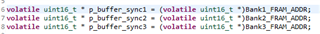
Customer used TI EVM TMDSRM48HDK. EMIF is connected with an onboard sdram and three asynchronous fram memories, and form the memory window, it is observed that the sdram reads and writes are OK, but the asynchronous access is not correct. 

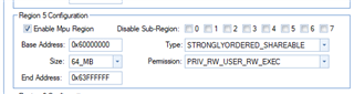
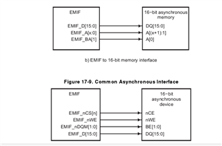
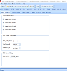
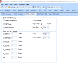
The following are the specific configurations:

The program code is as follows:

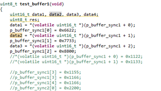
Read and write in test_buffer1() and the correct change can’t be seen in the storage monitor window. Then use an oscilloscope to monitor the write process for the ce, we pins and finally find that we pins are abnormal. The following is the diagram:

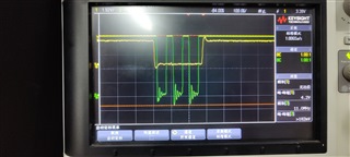
During a write cycle, the we pin changes repeatedly, and the customer would like to know if this is the cause of the write failure or if there are other problems with the asynchronous storage configuration.

Best Regards,

Cherry Zhou

  • Hi Cherry,

    This is HW bug. Please use the workaround in the device Errata: EMIF#4 Write to external asynchronous memory configured as “normal” causes extra WE pulse

    Workaround: External asynchronous memory must be configured to be "device" type or "stronglyordered" type using the CPU's MPU.

  • Hi QJ,

    Once the customer has configured this way, it still doesn't work, as shown in the following figure:

    Then the customer refers to the other response in the forum: The following statement is needed to initialize the mpu. There is no more one write, we flip over and over again.

    _mpuDisable_();
    _mpuInit_();
    _mpuEnable_();

    However, the write is still not successful, and the customer guesses that the following possible reasons are:

    (1) ASYNC initialization configuration is not right, which is generated automatically by halcogen. As shown below, the code generated by the customer's sdram operation using halcogen could not be read or written successfully, and the sdram read and write was no problem after referring to the previous initial code in the forum.

    void emif_ASYNC1Init(void)
    {
    /* USER CODE BEGIN (4) */
    /* USER CODE END */
    emifREG->CE2CFG = 0x00000000U;
    emifREG->CE2CFG = (uint32)((uint32)0U << 31U)|
    (uint32)((uint32)0U << 30U)|
    (uint32)((uint32)2U << 26U)|
    (uint32)((uint32)6U << 20U)|
    (uint32)((uint32)1U << 17U)|
    (uint32)((uint32)1U << 13U)|
    (uint32)((uint32)8U << 7U)|
    (uint32)((uint32)1U << 4U)|
    (uint32)((uint32)1U << 2U)|
    (uint32)((uint32)emif_16_bit_port);
    
    emifREG->AWCC = (emifREG->AWCC & 0xC0FF0000U)|
    (uint32)((uint32)emif_pin_high << 29U)|
    (uint32)((uint32)emif_pin_low << 28U)|
    (uint32)((uint32)emif_wait_pin0 << 16U)|
    (uint32)((uint32)0U);
    
    emifREG->PMCR = (emifREG->PMCR & 0xFFFFFF00U)|
    (uint32)((uint32)0U << 2U)|
    (uint32)((uint32)emif_4_words << 1U)|
    (uint32)((uint32)0U);
    /* USER CODE BEGIN (5) */
    /* USER CODE END */
    }

    (2) The pins are not wired. As shown in the diagram below, the customer would like to know that if EMIF_nDQM[1:0] must be connected to the fram? According to the fram-side application note, the two byte enable pins can be directly grounded if the 16-bit data mode is used.

    Best Regards,

    Cherry Zhou

  • (1) ASYNC initialization configuration is not right, which is generated automatically by halcogen. As shown below, the code generated by the customer's sdram operation using halcogen could not be read or written successfully, and the sdram read and write was no problem after referring to the previous initial code in the forum.

    The EMIF Async timing parameters should be programmed properly. Those parameters are determined based on the timing parameters in your FRAM spec.

    The pins are not wired.

    It is ok. 

    Do you follow the signal mapping in Figure 17-8?

    EMIF_ADDR[x,0] --- FRAM_ADDR[x+1, 1]

    EMIF_BA[1] --- FRAM_ADDR[0]