This thread has been locked.

If you have a related question, please click the "Ask a related question" button in the top right corner. The newly created question will be automatically linked to this question.

TMS570LC4357: Using Quad SPI with MIBSPI5

Part Number: TMS570LC4357

Is it possible to use a Quad SPI device connected to MIBSPI5.

I see they talk about parallel mode 2-2, 4-4, 8-8....

I have a  a S70FL01GS (dual 512Mbit) spi memory which I can run as 2 independent dies, or I can run it in quad mode...

just not sure if the "parallel mode" descirbed in the HERC ref manual (section 28.2.6.6.5...SPNU563A–March 2018)

appreciate the response as usual

thank you!

  • Hi,

    The serial Quad SPI protocol uses 4 pins (IO[3:0]) to send and then receive, which is half-duplex. The MibSPI in parallel uses 4 lines (SIMO[3:0]) to send and separate 4 line (SOMI[3:0]) to receive, that is full-duplex.

    To use S70FL01GS flash, you need to send the command/address/data trough 4 pins. There are predefined commands for writing, reading, and erasing operations. To covert full-duplex to half-duplex, you may need external circuitry to switch lines for send and receive.

  • TMS570LC3x doesn't support QSPI, but they support multi-buffered SPI in parallel mode (MibSPI in parallel). MibSPI in parallel is full-duplex communication, but QSPI is half-duplex.

    The communication protocols are also different:

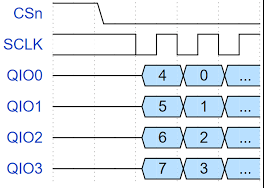
    1. QSPI: The following waveform is for charlen = 8-bit

    As you can see 4 bits are transferred every clock cycle. The bit order is QIO0 sends bit4, QIO1 sends bit5 and so on in the first clock cycle and bits 0,1,3, and 3 are sent out in the 2nd clock cycle.

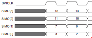
    2. MibSPI in parallel: The following waveform is for charlen=16-bit

    In 4-data line mode (master mode) the shift register bits 15, 11, 7, and 3 will be connected to the pins SIMO[3], SIMO[2], SIMO[1], and SIMO[0], and the shift register bits 12, 8, 4, and 0 will be connected to the pins SOMI[3], SOMI[2], SOMI[1], and SOMI[0]. The subsequent rising edge of SPICLK will shift data in the shift register by 1 bit to the left (SIMO[3] will shift the data out from bit 15 to 12, SIMO[2] will shift the data out from bit 11 to 8, SIMO[1] will shift the data out from bit 7 to 4, SIMO[0] will shift the data out from bit 3 to 0). After four SPICLK cycles, when the full data word is transferred, the shift register (16 bits) is copied to the receive buffer, and the RXINT flag will be set.

  • thank you very very much!