This thread has been locked.

If you have a related question, please click the "Ask a related question" button in the top right corner. The newly created question will be automatically linked to this question.

RM48L950: F021 Flash API Read and Write

Part Number: RM48L950
Other Parts Discussed in Thread: HALCOGEN

Hi TI,

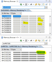
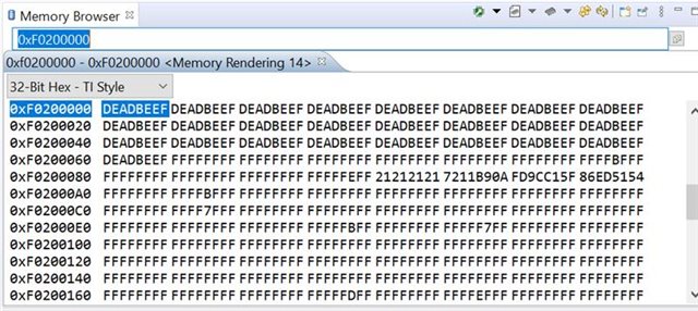
I'm trying to write and read the sector 7 (0xF0200000) of the the flash. I'm able to do it. but the issue is, the flash is not erasing properly even when loading the code for debug and executing erase function. after erasing it leaves behind some random junk values in the flash as shown in the below ss.

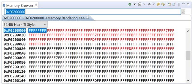
and sometimes the flash will not erase fully as shown in the below ss.

because of this issue, my data is corrupting sometimes while writing to the flash. what is the reason for this and how i can solve the error. can you please help me on this.

with regards,

Nagaraju M

  • Hi Nagaraju,

    The random non-F value in the first snapshot is caused by the invalid ECC value. When you erase the EEPROM flash sector, the EEPROM ECC space is also erased. EEPROM is protected by SECDED logic in the Flash wrapper. After erased, the content in ECC space is not a valid ECC value.

    The sector is not erased successfully. Did you get any error when erasing the flash? 

  • Hi Wang,

    During testing, we tried to erase EEPROM Sector No. 0 and 1. But, we didn't receive any error when erasing the EEPROM sector. 

    Also, after erasing the respective EEPROM sector,  then we tried to read and check at each address whether the data value is 0xFFFFFFFF, we found some non-F value, which is posted above. 

    What is the address and size of the EEPROM ECC space? Is there any solution for retrieving the erased ECC space?

    How to check whether the EEPROM sector is erased properly?

  • Hi Wang,

    as  said, we didn't get any error while erasing the EEPROM sector. we're noticed that, when we erased the flash. in sector0 and sector1 there are many non-F values are found. is there any solution to retrieve the erased ECC space? and what is the address and size of it?

    your response will be highly appreciated.

  • Hi,

    The flash wrapper has two buses, the bus1 and bus2.

    The bus1 is used by the CPU to access the flash's normal sectors (bank 0 and bank 1) for which the program and data are stored. The CPU will use the bus2 to access the OTP sectors, EEPROM emulation flash bank. 

    When CPU accesses program flash (bank 0 and bank 1)  via bus1, the CPU's built-in SECDED logic will perform the ECC checking. Note this ECC logic is inside the CPU, not inside the flash wrapper. 

    When CPU accesses the EEPROM and OTP sectors, the ECC checking is done inside the flash wrapper. The reason is that the CPU's level 2 interface (AXI-M bus) which is connected to the flash memory system's bus2 does not have ECC checking capability. Therefore, the flash wrapper has its own ECC logic just for bus2 accesses.

    The ECC checking inside the flash wrapper is not enabled by default. if it is not enabled, your will not get error when reading the erased EEPROM, so the read out value is 0xFFFFFFFF.

    If you enable the ECC by writing 0x0A to EE_EDACEN bit field of EE_CTL1 register, you will see non-F byte when reading the erased EEPROM.

  • When the ECC is enabled (bit[3:0] = 0xA of EE_CTRL1, address is 0xFFF8308) , you can see the non-F bytes in first memory window:

  • Thank you so much for your detailed response.

  • Hi wang, 

    Below are some doubts. 

    1. Is it recommended to disable the ecc correction when we need to do R/W from emulated eeprom?

    2. Is there any function available to do ECC disable in Flash API? Like you suggested with memory browser?

    3. Whether we can store the data in EEPROM_SECTOR_2?

    Regards, 

    Monish

  • Hi Monish,

    My suggestion is to use FEE driver to program data to Bank 7 (emulated EEPROM).

    EEPROM allows users to erase and reprogram stored data repeatedly in an application. The TI FEE Driver provides a set of software functions intended to use a Sector of on-chip Flash memory (Bank 7) as the emulated EEPROM. These software functions are transparently used by the application program for writing, reading and modifying the data.

    Please read the user guide in HalCoGen installation folder:

    TI FEE User Guide.pdf

    The HALCoGen has an example for  EEPROM reading/writing using FEE driver: