This thread has been locked.

If you have a related question, please click the "Ask a related question" button in the top right corner. The newly created question will be automatically linked to this question.

TM4C123AH6PM: GPIO pad damage

Part Number: TM4C123AH6PM

Hello all,

We have one application that uses a TM4C123AH6PM. One of the GPIO's is connected to the gate of a N-ch mosfet which controls a power line.

The EN_5V_BOOST_PWR is connected directly to GPIO PB3, pin #48 of the IC. There is no other connection on this signal - one end in the MCU, the other in the gate.

The pad is configured as output, 4mA, standard.

Over the past months we've had several failures on this GPIO. When that happens, the voltage out of the MCU no longer goes above ~1.2V. It goes to zero if the pin is set low, but when set high it won't reach the expected 3V3.

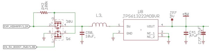
Schematic is shown above. The issue has happened in several different boards, different MCU batches, but the symptom is always the same. And the only solution is to replace the MCU.

It does seem to be a hardware issue with a lot of possible guesses, but such a simple design leaves us little inspiration to look for reasons - so we are reaching out here for ideas of where to look.

Regards

Bruno

  • Hello Bruno,

    To help understand some further context behind the design / start troubleshooting this issue:

    1. Is this a new design, or an existing design that only began to show issues recently?
    2. If an existing design, were there any part changes that are relevant to this part of the schematic?
    3. Has the GPIO#10 errata been considered for investigation?
    4. When the I/O is at ~1.2V, what is the current draw measured?
    5. When the MCU is swapped, if the failing MCU is placed on another board, does the issue follow the MCU?
      1. Also, once swapped, is the issue essentially permanently resolved, or do the same boards eventually have the failure again?

    Best Regards,

    Ralph Jacobi

  • Hi Ralph, thanks for the strategic pointers!

    1. This is a new design, second iteration of the board, only a few prototypes running over the last six months.

    2. No relevant changes - using a N/P dual mosfet to control power lines is something that we do very often (with the very same Q6 which is SI3585CDV-T1-GE3) and I have never seen this failure mode before. Reminding here that the GPIO is connected to the GATE, which is pretty much high impedance.

    3. I took a look and it does not seem to apply here. The pin itself is output, and even if a neighbor were to blame, the reconfiguration of the pad does not solve it.

    4 and 5: This needs more testing. What I remember having done is to unsolder/lift the MUC's GPIO away from the board and: on the MCU side, the behavior was still the same "max 1.2V" when enabled - and on the board side, applying 3V3 directly into the mosfet gate will turn it on as expected.

    Regards,

    Bruno

  • Hi Bruno,

    Looking at the D/S for the FET in question, it looks like the impendence of the Gate is lower at high frequency. How fast is the switching being done? Is the switching being done faster on this board than others?

    I was talking over this with Charles and we both would like to understand the current measurements for various scenarios

    • Current of I/O at 1.2V during failure
    • Current of I/O at 1.2V while not connected to FET
    • Current of I/O under normal operation on a working board

    Also what current setting have you applied to the GPIO register? I'm guessing this is configured in push-pull with a weak pull down resistor?

    FYI 1.2V is the VDDC level in the device so it almost feels like the failed pin is being clamped to VDDC which is quite unusual behavior. It is strange that the high is going to 1.2V only because usually I would think it would be pulling it low is clamping at 1.2V as it hits the max current draw. So this is kind of inverse of when I'd expect such a behavior to occur. 

    Best Regards,

    Ralph Jacobi