This thread has been locked.

If you have a related question, please click the "Ask a related question" button in the top right corner. The newly created question will be automatically linked to this question.

TM4C123GH6PZ: damaged parts using DFU

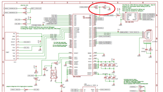
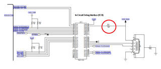
Part Number: TM4C123GH6PZ
Other Parts Discussed in Thread: TPS2051B

Hi, I'm using tm4c123gh6pz on custom boards and programming them troguh usb port with LM flash programmer DFU and ROM bootloader and I getting some parts damaged or heated.

I have connected D+ to PJ1, D- to PJ0, VBUS to PB1 and ID to PB0.

As I unserstand it could be caused by PB1 when configured as GPIO(default), so should I power up the board with the virgin microcontroller first to let the bootloader start and then conect the USB cable?

also it is necesary that ID pin is conected for DFU? if not, can cause problems if I left it conected to PB0?

Regards

Rafael

  • Hi Rafael,

      Please make sure when configured as GPIO, the PB0 and PB1 pins are limited to 3.6V as these two pins are not 5V tolerant. When PB0 and PB1 are used as USB functions they must remain in the respective USB pin mode configurations to prevent device damage.

    10.1 Signal Description
    GPIO signals have alternate hardware functions. The following table lists the GPIO pins and their
    analog and digital alternate functions. All GPIO signals are 5-V tolerant when configured as inputs
    except for PD4, PD5, PB0 and PB1, which are limited to 3.6 V. The digital alternate hardware functions
    are enabled by setting the appropriate bit in the GPIO Alternate Function Select (GPIOAFSEL)
    and GPIODEN registers and configuring the PMCx bit field in the GPIO Port Control (GPIOPCTL)  

    also it is necesary that ID pin is conected for DFU? if not, can cause problems if I left it conected to PB0?

    I don't think DFU mode requires the ID signal. 

  • ok, so if I limit PB1 to 3.6 permanently VBUS can work? or how could I do it only when in GPIO mode?

    another thing I have doubt, from the ROM user guide I can notice that the device is configured as self-powered, does it mean that the microcontroller provide VBUS?

    thanks for your help!

  • ok, so if I limit PB1 to 3.6 permanently VBUS can work? or how could I do it only when in GPIO mode?

    What I'm saying is that if you are going to use PB1 pin as a GPIO, not VBUS function then you need to limit the voltage to no more than 3.6V. 

    another thing I have doubt, from the ROM user guide I can notice that the device is configured as self-powered, does it mean that the microcontroller provide VBUS?

    If the device is self-powered, it means there should be a power source on your board to supply power to the device. If the device is bus-powered, then VBUS from the USB connector supplies power to your regulator. 

    Below is from USB library user's guide. 

    If an application only needs to run in device mode there are two options to control how device
    mode is entered. The USBStackModeSet() function is still used to control device mode operation.
    The application uses eUSBModeForceDevice when the application needs to free up the VBUS
    and ID pins or does not want VBUS to be monitored. The impact of this is that the application is
    not informed of USB disconnection events because it can no longer monitor VBUS. This is only a
    problem for self powered applications and can be handled by monitoring VBUS on a separate pin. If
    the application needs to receive disconnect events it uses the eUSBModeDevice setting and must
    connect the VBUS pin to the USB connector and leave the ID pin unconnected.

    Below is from the datasheet. 

    Note: When used in OTG mode, USB0VBUS and USB0ID do not require any configuration as they
    are dedicated pins for the USB controller and directly connect to the USB connector's VBUS
    and ID signals. If the USB controller is used as either a dedicated Host or Device, the
    DEVMODOTG and DEVMOD bits in the USB General-Purpose Control and Status
    (USBGPCS) register can be used to connect the USB0VBUS and USB0ID inputs to fixed
    levels internally, freeing the PB0 and PB1 pins for GPIO use. For proper self-powered Device
    operation, the VBUS value must still be monitored to assure that if the Host removes VBUS,
    the self-powered Device disables the D+/D- pull-up resistors. This function can be
    accomplished by connecting a standard GPIO to VBUS.

  • is there something that I can do? since I already have the PCBs done I can't conect VBUS to other pin, I see in the schematic of the launchpad of tm4c123 and tm4c1294 diferent circuits for PB1.

  • Hi,

      You should have at least a 100ohm series resistor if you are going to use the USB in a Device-Only mode. Please refer to section 4.1.1. of the TM4C123 System Design Guideline. https://www.ti.com/lit/pdf/spma059

    4.1.1 USB Device Only
    For TM4C123x devices that are used in a device-only configuration, the only signal used in addition to
    USB0DM and USB0DP is USB0VBUS, which is located on port PB1. In USB device-only mode,
    USB0VBUS is used to detect when voltage has been applied to or removed from the USB connector,
    which triggers software to manage the internal USB PHY accordingly. When configured as USB0VBUS,
    this pin is 5-V tolerant. However, when used as a GPIO input, PB1 is NOT 5-V tolerant. An alternate 5-V
    tolerant Fail-Safe GPIO should be selected to do the VBUS detection if there is a chance 5V could be
    applied to the input prior to PB1 on the TM4C123x device being configured for VBUS, such as during
    power-up, while the device is in reset, and the while the initial boot sequence executes.
    For a USB device-only configuration, a 100Ω resistor should be placed in series between VBUS on the
    USB connector and PB1 (or alternate 5-V tolerant GPIO) on the microcontroller in order to limit damage
    caused by any ESD events.
    If PB1 must be used for a function other than USB0VBUS, any other available 5-V tolerant Fail-Safe GPIO
    could be used in its place.


    4.1.2 USB Embedded Host
    For TM4C123x devices that are used in a host-only configuration, the USB0EPEN and USB0PFLT signals
    may be used in the design in addition to USB0DM and USB0DP. These two signals typically connect to a
    power switch such as a TPS2051B, which controls power to the host's USB connector. Refer to the
    TM4C123x device's data sheet to determine which ports these functions are available on.


    4.1.3 USB OTG
    TM4C123x devices that support USB OTG mode include the signals for USB Device mode, signals for
    USB Host mode and an additional signal USB0ID located on pin PB0. This USB ID signal is the 5th pin
    found on a USB micro-AB connector. If a micro-A cable end is plugged into this connector, the ID pin on
    the cable is tied to ground causing the TM4C123x device to operate as a USB host. If a micro-B cable end
    is plugged into the USB connector, the ID pin is left floating. In this case, the TM4C123x device's internal
    pull-up on the USB0ID signal causes the controller to operate in device mode.
    In order to limit damage from ESD events, a 100Ω resistor should be placed in series between the ID pin
    on the USB connector and USB0ID(PB0) on the microcontroller.
    To support full USB OTG negotiation using the SRP and HNP protocols, VBUS from the USB connector
    must be directly connected to USB0VBUS(PB1) of the microcontroller without a series resistor in between.
    In this case, USB0VBUS should be connected to an ESD suppressor such as a TVS diode, or ESD
    resistant VBUS switch. PB1 on the TM4C123x family devices is not 5V tolerant until after PB1 has been
    configured for its USB0VBUS function. Until this configuration point (during power-up, while in reset and
    the during the initial boot sequence) the input voltage on PB1 must not exceed the voltage on VDD + 0.3V.