Part Number: TMS570LS0332
Hi,
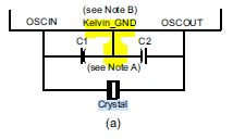
I cannot find in the datasheet if the Kelvin GND of the uC can/shall be connected to the ground of the UC.
Do you have also a layout guideline for the crystal for best inmunity? Should we have a local ground for this kelvin connection?