This thread has been locked.

If you have a related question, please click the "Ask a related question" button in the top right corner. The newly created question will be automatically linked to this question.

TM4C1290NCPDT: The rise and fall time specification about input terminal (GPIO and UART)

Part Number: TM4C1290NCPDT

Hi Experts

Regarding UART (Rx) and GPIO is set Input,

How much the rise time and fall time are allowed for UART (Rx) and GPIO (Input) ?
I couldn't find the upper limit as the rise and fall time on the datasheet.

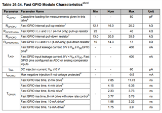
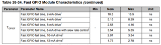
The following characteristics on the datasheet (Rev B, page 1592 - 1593).
the characteristics is set GPIO as output, right?

  • Hello,

    How much the rise time and fall time are allowed for UART (Rx) and GPIO (Input) ?

    For a GPIO it would not make sense to characterize an input maximize rise time. The idea of the characterization of the output rise and fall times is to give a system designer an understanding of the worst case scenario for a signal controlled by the TM4C MCU to change. An external signal can behave however it wants and the system designer needs to take into account the rise or fall time from the output of the external device when determining how the TM4C MCU should react to the changing signal.

    From a serial peripheral communication standpoint, the rise and fall times are governed by the selected data rate more than anything. For higher speed interfaces like SSI and I2C, some specifications are given to ensure the bus moves slowly enough to register data, but if the bus took longer to have signals rise and fall that just impacts the actual data rate of the transfer and again it is up to the system designer to account for that. In the event of a slave device responding to a provided clock signal too slowly, then the result would be missing data, but it would not be due to a characterized 'upper limit' for the rise and fall time but rather that the signal was not changed in time for the latching on a clock edge which will be consistently output as part of the data rate selected. Therefore it is the clock speed plus any specified valid/setup/hold times which governs the upper limits for proper operation with the clock speed being a variable based on system specific configuration.

    In summary, the 'upper limit' of rise/fall times for an external signal that is input into the TM4C is not a specification that can be characterized universally as it is application and system specific and needs to be determined by the system designer based on expected performance.

    Best Regards,

    Ralph Jacobi

  • Hi Jacobi-san

    Thanks to quickly answer.

    I undaestand that your answer means "The MCU is not damaged and destroied by through current on input terminal (GPIO input, UART Rx)", right?

  • Hello,

    Rise / Fall time maximums does not correlate to current injection on the I/O.

    We have those limits clearly specified in the datasheet in Section 26.3.2.1 GPIO Current Restrictions as the current input allowed is based on each side of the MCU.

    The table does have a small issue in that the listing for the 'Bottom side' package pins is not fully accurate for the TM4C1290NCPDT device and it should be following: PA[0-7], PF[0-4],PG[0-7], PK[4-7], PQ[5-6]

    Best Regards,

    Ralph Jacobi

  • Hi Jacobi-san

    I found the comment  " All digital inputs are Schmitt triggered"  on specification.

    It's means that If  the MCU input terminal (GPIO input, UART Rx) is allowed to input the signal with slow rise and fall time (ex, 60Hz sine wave).

    If so, my quiestion is resolved.

  • Hello,

    Yes that is the case. All pins configured as digital inputs are Schmitt-triggered and do not have slow rise and fall time limitations.

    Best Regards,

    Ralph Jacobi