This thread has been locked.

If you have a related question, please click the "Ask a related question" button in the top right corner. The newly created question will be automatically linked to this question.

TMS570LS3137: nDQM signals issue while interfacing EMIF to FPGA on 8bit bus

Part Number: TMS570LS3137
Other Parts Discussed in Thread: HALCOGEN

Dear all,

My board has an FPGA connected to EMIF_nCS2 (async device 1, mapped at 0x60000000 memory address) of the TMS570LS3137 EMIF interface.
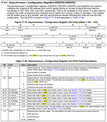
I set up the peripheral via HalCoGen with 8 bit data bus, select strobe mode, and extended wait.

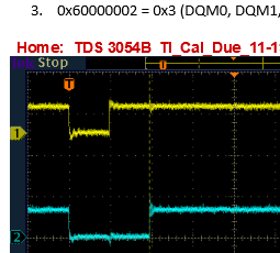
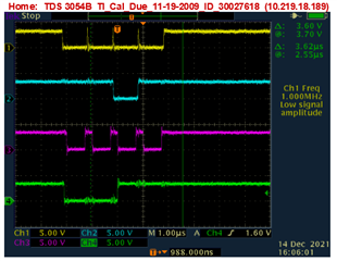
When I read 8 bit variables starting from address 0x60000000 I can see that the first 2 reads have correct EMIF_ADDR, correct EMIF_BA[1:0], correct EMIF_nCS2 and correct EMIF_nDQM[1:0] signals.
The third read, the one with EMIF_BA[1:0] = 0b10 has bad EMIF_nDQM signals: both bits to 0.
This condition is not vaild, thus the FPGA publics 0x00 on the data bus. The picture below shows the signals on the data bus


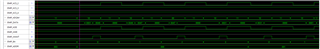
This issue appears every time the EMIF_BA[1:0] equals 0b10.

I read that the mpu should set that address segment as DEVICE type on some forums but this doesn't seem to resolve the problem.
Any advice for configuring the EMIF peripheral?

Thanks in advance,
Federico Gobetti.

  • Hi Federico,

    For 8-bit bus, for each nCS and nOE active phase, only 1 byte is transferred (read or write). In your diagram, where are there 2 bytes for each transaction? 

    1. address offset:0x00 --- data= 0x0001, 0x0049, DQM[1:0]=b10

    2. address offset:0x01 ---data= 0x0049, 0x0047, DQM[1:0]=b10

  • Hi Federico,

    The DQM signals toggle depending on the size of the access and the size of the EMIF bus.

    For example, if EMIF bus is16-bits in size and you perform a 32-bit access. you will see two 16-bit accesses on the bus with both DQM pins asserted (low). If your access is 8 bits, then DQM0 will go low if the LSB of the address is 0 or DQM1 will go low if the LSB is 1.  

    If EMIF bus is 8-bit in size, then only DQM0 should toggle and it will toggle for every access.

  • Hi QJ, thanks for you attention.

    I think I need to be more precise. I have a 8-bit bus and I'm reading 8-bit registers, thus I expect 1 transaction (nCS, nOE active phase) per read.
    Data are ready at rising edge of nWAIT
    In my diagram you can see:

    • 1st read - address offset:0x00, nDQM[1:0]=b10, data= 0x0049

    • 2nd read - address offset:0x01, nDQM[1:0]=b10, data= 0x0047

    • 3rd read - address offset:0x02, nDQM[1:0]=b00, data= 0x0000 (should be 0x0057)

    • 4th read - address offset:0x03, nDQM[1:0]=b10, data= 0x0031

    The third read has BAD data, because the FPGA cannot update the data bus while nDQM are both low during a 8-bit transaction.
    This faulty condition repeats itself everytime the less significative bits of the address offset are 0b10, thus at address 0x02, 0x06, 0x0A... and so on...
    The image below adds more details:


    It looks to me as if EMIF tries to make a 16-bits access to those peculiar addresses, so it enables both nDQM signals.

  • It looks to me as if EMIF tries to make a 16-bits access to those peculiar addresses, so it enables both nDQM signals.

    Can you use the debugger to read back the CE2CFG register, named Async1Cfg in the CCS device registers, and check the ASIZE field is set to zero to confirm an 8-bit data bus has seen set?

  • Hi Chester,

    the CE2CFG register is set (by the HalCogen generated emif_ASYNC1Init() function) to:

    emifREG->CE2CFG =   (uint32)((uint32)1U << 31U)|
                        (uint32)((uint32)1U << 30U)|
                        (uint32)((uint32)0U << 26U)|
                        (uint32)((uint32)1U << 20U)|
                        (uint32)((uint32)0U << 17U)|
                        (uint32)((uint32)0U << 13U)|
                        (uint32)((uint32)1U << 7U)|
                        (uint32)((uint32)0U << 4U)|
                        (uint32)((uint32)1U << 2U)|
                        (uint32)((uint32)emif_8_bit_port);


    The debugger confirms the expected value: 0xC0100084


  • Hi Federico,

    As I mentioned, for EMIF bus is 8-bit in size, only DQM0 should toggle and it will toggle for every access, and DQM1 is "don't care"

    I also noticed that the DQM1 is toggled to LOW when the address offset is 0x2.

    You may use other signals for FPGA to update the data bus.

  • The first channel is DQM0, the 2nd channel is DQM1, the 3rd channel is nWE, and the 4th channel is a GIO signal.

    The EMIF BUS width is 8 bit,

    Four writes:

    uint8_t *sram_ptr = (uint8_t *)0x60000000;

    *sram_ptr++ = 0x1;
    *sram_ptr++ = 0x2;
    *sram_ptr++ = 0x3;
    *sram_ptr++ = 0x4;

  • I also noticed that the DQM1 is toggled to LOW when the address offset is 0x2.

    Is that something which should be noted in the TRM, or described in the device errata?

  • This is one more confirm to what I saw on the bus. 
    I will ignore DQM1 signal for 8 bit data.

    Thank you,
    Federico Gobetti